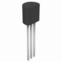
TC54VN4502EZB Microchip Technology, TC54VN4502EZB Datasheet - Page 2

TC54VN4502EZB
Manufacturer Part Number
TC54VN4502EZB
Description
IC VOLT DET N-CH ODRN 4.5V TO92
Manufacturer
Microchip Technology
Type
Simple Reset/Power-On Resetr
Datasheet
1.TC54VN2102ECB713.pdf
(16 pages)
Specifications of TC54VN4502EZB
Operating Temperature
-40°C ~ 85°C
Number Of Voltages Monitored
1
Output
Open Drain or Open Collector
Reset
Active Low
Voltage - Threshold
4.5V
Mounting Type
Through Hole
Package / Case
TO-92-3 (Standard Body), TO-226
Threshold Voltage
4.5V
No. Of Supervisors / Monitors
1
Supply Voltage Range
0.7V To 10V
Supply Current
1.1µA
Delay Time
200µs
Digital Ic Case Style
TO-92
No. Of Pins
3
Reset Type
Active-Low / Push-Pull
Rohs Compliant
Yes
Lead Free Status / RoHS Status
Lead free / RoHS Compliant
Reset Timeout
-
Lead Free Status / RoHS Status
Lead free / RoHS Compliant
Other names
158-1087
158-1087
Q1566849
Q3445532
158-1087
Q1566849
Q3445532
TC54
1.0
Absolute Maximum Ratings †
Input Voltage ...................................................................+12V
Output Current ..............................................................50 mA
Output Voltage: CMOS................(V
Power Dissipation (T
Operating Temperature Range........................-40°C to +85°C
Storage Temperature Range .........................-65°C to +150°C
DC CHARACTERISTICS
DS21434H-page 2
Electrical Specifications: Unless otherwise noted, T
Operating Voltage
Quiescent Current
Threshold Voltage
(Note 1)
Hysteresis Voltage
Output Current
Tempco of (V
Delay Time
Note 1:
3-Pin SOT-23A .......................................................240 mW
3-Pin SOT-89..........................................................500 mW
5-Pin SOT-23A .......................................................240 mW
3-Pin TO-92 ............................................................300 mW
Parameter
ELECTRICAL
CHARACTERISTICS
For other voltage options, please contact your regional Microchip sales office.
DET
Open-Drain.....................(V
–)
A
≤ 70°C):
T
C
V
V
(V
Sym
I
t
DET
V
HYST
I
OUT
DLY
SS
IN
DET
SS
–
– )
– 0.3V) to (V
SS
1.37
2.06
2.65
2.84
2.94
4.12
4.21
Min
0.7
0.7
3.0
5.0
6.0
7.0
28
42
54
58
60
84
86
– 0.3V) to 12V
—
—
—
—
—
—
—
IN
+ 0.3V)
A
= +25°C.
-10.0
±100
10.1
11.5
13.0
Typ
105
135
145
150
210
215
0.8
0.9
1.0
1.1
1.4
2.1
2.7
2.9
3.0
4.2
4.3
7.7
70
—
—
—
Max
10.0
1.43
2.14
2.75
2.96
3.06
4.28
4.39
168
216
232
240
336
344
-2.0
112
6.0
2.7
3.0
3.2
3.6
0.2
—
—
—
—
—
† Stresses above those listed under "Absolute Maximum
Ratings" may cause permanent damage to the device. These
are stress ratings only and functional operation of the device
at these or any other conditions above those indicated in the
operation sections of the specifications is not implied.
Exposure to Absolute Maximum Rating conditions for
extended periods may affect device reliability.
ppm/°C -40°C ≤ T
Units
mV
mA
µA
ms
V
V
V
(V
(V
V
V
V
V
TC54VX14
TC54VX21
TC54VX27
TC54VX29
TC54VX30
TC54VX42
TC54VX43
V
V
V
V
V
V
V
V
V
V
V
TC54VC Only:
V
V
IN
IN
IN
IN
DET
DET
DET
DET
DET
DET
DET
OL
OL
OL
OL
OH
DET
DET
DET
= 2.0V
= 3.0V
= 4.0V
= 5.0V
= 0.5V, V
= 0.5V, V
= 0.5V, V
= 0.5V, V
= V
– → V
= 1.4V (typical)
= 2.1V (typical)
= 2.7V (typical)
= 2.9V (typical)
= 3.0V (typical)
= 4.2V (typical)
= 4.3V (typical)
– ) ≥ 1.6V
– ) < 1.6V
IN
© 2007 Microchip Technology Inc.
A
– 2.1V, V
≤ 85°C
OUT
Test Conditions
IN
IN
IN
IN
= 2.0V
= 3.0V
= 4.0V
= 5.0V
inversion
IN
= 8.0V


