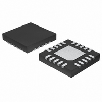
MAX16042TP+ Maxim Integrated Products, MAX16042TP+ Datasheet - Page 3

MAX16042TP+
Manufacturer Part Number
MAX16042TP+
Description
IC SUPERVISOR CIRC TRPL 20TQFN
Manufacturer
Maxim Integrated Products
Type
Sequencerr
Datasheet
1.MAX16041TE.pdf
(15 pages)
Specifications of MAX16042TP+
Number Of Voltages Monitored
3
Output
Push-Pull, Totem Pole
Reset
Active Low
Reset Timeout
140 ms/Adjustable Minimum
Voltage - Threshold
9 Selectable Threshold Combinations
Operating Temperature
-40°C ~ 125°C
Mounting Type
Surface Mount
Package / Case
20-TQFN Exposed Pad
Undervoltage Threshold
Adjustable
Overvoltage Threshold
Adjustable
Manual Reset
Resettable
Watchdog
No Watchdog
Supply Voltage (max)
28 V
Supply Voltage (min)
2.2 V
Supply Current (typ)
52 uA
Maximum Power Dissipation
2051 mW
Maximum Operating Temperature
+ 125 C
Mounting Style
SMD/SMT
Minimum Operating Temperature
- 40 C
Lead Free Status / RoHS Status
Lead free / RoHS Compliant
ELECTRICAL CHARACTERISTICS (continued)
(V
Note 1: Devices are production tested at T
Note 2: Operating below the UVLO causes all outputs to go low. The outputs are guaranteed to be in the correct state for V
Note 3: To guarantee an assertion, the minimum input pulse width must be greater than 2µs.
CRESET AND CDLY_
CRESET Threshold
CRESET Charge Current
CDLY_ Threshold
CDLY_ Charge Current
DIGITAL LOGIC INPUTS (EN_, MR, TOL, TH1, TH0)
Input Low Voltage
Input High Voltage
TH1, TH0 Logic-Input Floating
TOL, TH1, TH0 Logic-Input
Current
EN_ Input Leakage Current
MR Internal Pullup Current
OUTPUTS (OUT_, RESET)
Output Low Voltage
(Open-Drain or Push-Pull)
Output High Voltage (Push-Pull)
Output Leakage Current
(Open-Drain)
Reset Timeout Period
TIMING
IN_ to OUT_ Propagation Delay
IN_ to RESET Propagation Delay
MR Minimum Input Pulse Width
EN_ or MR Glitch Rejection
EN_ to OUT_ Delay
MR to RESET Delay
CC
= 2.2V to 28V, T
to 1.2V.
Adjustable, Sequencing/Supervisory Circuits
PARAMETER
_______________________________________________________________________________________
A
= -40°C to +125°C, unless otherwise specified. Typical values are at V
Dual-/Triple-/Quad-Voltage, Capacitor-
t
V
I
SYMBOL
V
RST-DELAY
I
CH-RESET
CH-CDLY
t
TH-RESET
t
TH-CDLY
DELAY+
DELAY-
V
I
t
V
t
V
LKG
t
V
OFF
ON
RP
OH
OL
IH
IL
A
= +25°C. Limits over temperature are guaranteed by design.
CRESET rising, V
V
CDLY_ rising, V
V
V
V
V
V
V
V
V
V
Output not asserted low, V
CRESET = V
CRESET open
IN_ rising, CDLY_ open
IN_ falling, CDLY_ open
CRESET open, IN_ falling
(Note 3)
From device enabled to device disabled
From device disabled to device enabled
(CDLY_ open)
MR falling
CC
CC
TOL
EN_
CC
CC
CC
CC
CC
CC
= 3.3V
= 3.3V
= 3.3V
≥ 1.2V, I
≥ 2.25V, I
≥ 4.5V, I
≥ 3V, I
≥ 4.5V, I
, V
= V
TH1
CC
, V
SOURCE
or GND
CC
SINK
SINK
SOURCE
TH0
SINK
CONDITIONS
, V
CC
CC
CC
= GND or V
= 90µA
= 1mA
= 3.3V
= 0.5mA
= 500µA
= 3.3V
= 3.3V
= 800µA
OUT
CC
= 28V
CC
0.8 x V
0.8 x V
= 3.3V and T
0.465
0.95
-100
MIN
380
200
250
140
1.4
-1
2
CC
CC
0.030
TYP
500
250
535
190
280
0.5
0.6
35
20
35
30
1
3
3
A
= +25°C.) (Note 1)
0.535
+100
MAX
1.05
0.35
620
300
820
260
0.4
0.3
0.3
+1
1
CC
UNITS
ms
nA
nA
µA
nA
nA
µA
µs
µs
µs
ns
µs
µs
down
V
V
V
V
V
V
V
3


