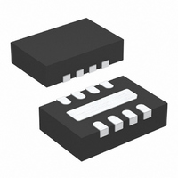
LTC2912CDDB-3#TRPBF Linear Technology, LTC2912CDDB-3#TRPBF Datasheet - Page 6

LTC2912CDDB-3#TRPBF
Manufacturer Part Number
LTC2912CDDB-3#TRPBF
Description
IC VOLT MONITOR SNGL 8-DFN
Manufacturer
Linear Technology
Type
Simple Reset/Power-On Resetr
Datasheet
1.LTC2912CTS8-1TRMPBF.pdf
(12 pages)
Specifications of LTC2912CDDB-3#TRPBF
Number Of Voltages Monitored
1
Output
Open Drain or Open Collector
Reset
Active High
Reset Timeout
Adjustable/Selectable
Voltage - Threshold
Adjustable/Selectable
Operating Temperature
0°C ~ 70°C
Mounting Type
Surface Mount
Package / Case
8-DFN
Lead Free Status / RoHS Status
Lead free / RoHS Compliant
Available stocks
Company
Part Number
Manufacturer
Quantity
Price
LTC2912
PIN FUNCTIONS
OV (Pin 6/Pin 3, LTC2912-3): Overvoltage Logic Output.
Asserts high with a weak internal pull-up to V
VL input is above threshold. Latches high. May be pulled
above V
unused.
TMR (Pin 4/Pin 5): Reset Delay Timer. Attach an external
capacitor (C
delay time of 9ms/nF . A 1nF capacitor will generate an
8.5ms reset delay time. Tie pin to V
UV (Pin 7/Pin 2): Undervoltage Logic Output. Asserts low
when the VH input voltage is below threshold. Held low for
a programmed delay time after the VH input is valid. Pin
has a weak pull-up to V
using an external pull-up. Leave pin open if unused.
6
BLOCK DIAGRAM
CC
using an external pull-up. Leave pin open if
TMR
2
3
5
VH
VL
GND
) of at least 10pF to GND to set a reset
0.5V
–
+
–
+
CC
and may be pulled above V
(DFN/TSOT Packages)
UVLO
UVLO
CC
to bypass timer.
1
V
CC
+
–
CC
when the
2V
V
CC
LTC2912-1, LTC2912-3
LTC2912-2
CC
V
GND with a 0.1μF (or greater) capacitor. Operates as a
direct supply input for voltages up to 6V. Operates as a
shunt regulator for supply voltages greater than 6V and
should have a resistance between the pin and the supply
to limit input current to no greater than 10mA. When used
without a current-limiting resistance, pin voltage must
not exceed 6V.
VH (Pin 2/Pin 7): Voltage High Input. When the voltage
on this pin is below 0.5V, an undervoltage condition is
triggered. Tie pin to V
VL (Pin 3/Pin 6): Voltage Low Input. When the voltage on
this pin is above 0.5V, an overvoltage condition is triggered.
Tie pin to GND if unused.
CC
(Pin 1/Pin 8): Supply Voltage. Bypass this pin to
DISABLE
DISABLE
CLEAR/BYPASS
OSCILLATOR
GENERATOR
GENERATOR
UV PULSE
OV PULSE
OV LATCH
4
TMR
+
–
–
+
1V
1V
LTC2912-1
LTC2912-2
LTC2912-3
CC
if unused.
V
V
CC
CC
400k
400k
LATCH
OV/OV
2μA
DIS
UV
7
6
8
8
2912 BD
2912fa


