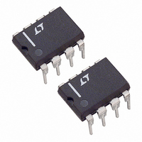
LTC1232CN8 Linear Technology, LTC1232CN8 Datasheet - Page 6

LTC1232CN8
Manufacturer Part Number
LTC1232CN8
Description
IC MPU SUPERVISORY CIRCUIT 8-DIP
Manufacturer
Linear Technology
Type
Simple Reset/Power-On Resetr
Datasheet
1.LTC1232CS8PBF.pdf
(8 pages)
Specifications of LTC1232CN8
Number Of Voltages Monitored
1
Output
Open Drain, Open Drain
Reset
Active High/Active Low
Reset Timeout
250 ms Minimum
Voltage - Threshold
4.37V, 4.62V
Operating Temperature
0°C ~ 70°C
Mounting Type
Through Hole
Package / Case
8-DIP (0.300", 7.62mm)
Lead Free Status / RoHS Status
Contains lead / RoHS non-compliant
Available stocks
Company
Part Number
Manufacturer
Quantity
Price
Part Number:
LTC1232CN8
Manufacturer:
LT/凌特
Quantity:
20 000
Part Number:
LTC1232CN8#PBF
Manufacturer:
LINEAR/凌特
Quantity:
20 000
APPLICATIO S I FOR ATIO
LTC1232
PI FU CTIO S
RST: Open Drain Logic Output for µP Reset Control.
The LTC1232 provides three ways to generate µP reset.
First, when V
TOL = GND and 4.5V with TOL = V
After V
RST to remain active low for a minimum of 250ms.
Second, when the watchdog timer is not serviced prior to
a selected time-out period, the reset pulse generator also
forces RST to active low for a minimum of 250ms and
repeats for every time-out period. Third and the last, when
the PB RST pin stays active low for a minimum of 40ms,
RST becomes active low. The RST output will remain
Power Monitoring
The LTC1232 uses a bandgap voltage reference and a
precision voltage comparator, C1, to monitor the 5V
supply input on V
below the V
TOL = GND and 4.37V typical with TOL V
outputs are forced to active states. The V
accounts for a 5% or 10% variation on V
outputs become active when V
point. On power-up, the reset signals are held in active
states for a minimum of 250ms after the V
reached to allow the power supply and microprocessor
to stabilize. On power-down, the RST signal remains
active low even with V
hold the microprocessor in stable shutdown condition.
Figure 1 shows the timing diagram of the RST signal.
6
U
CC
returns to 5V, the reset pulse generator forces
U
CC
CC
falls below V
CC
U
trip point (4.62V typical with
U
(see Block Diagram). When V
CC
as low as 1V. This capability helps
U
CC
CC
RST
V
CC
CC
falls below the V
V2
trip point (4.75V with
), RST goes active low.
W
CC
t 1
CC
CC
, so the reset
CC
), the reset
trip point is
U
Figure 1. Reset Active Time
trip point
CC
CC
falls
trip
V1
V2
active low for a minimum of 250ms from the moment the
push-button reset input is released from logic low level.
RST: RST is an Active High Logic Output. It is the inverse
of RST.
ST: Logic Input to Reset the Watchdog Timer. Driving ST
either high or low longer than the time-out period set by
the TD input, forces the reset outputs to active states for
a minimum of 250ms. The timer resets itself and begins to
time-out again with each high to low transition on the ST
input (see Figure 2).
The precision voltage comparator, C1, typically has 40mV
of hysteresis which ensures that glitches at V
activate the reset outputs. Response time is typically 10µs.
To help prevent mitriggering due to transient loads, V
pin should be bypassed with a 0.1µF capacitor with the
leads trimmed as short as possible.
Push-Button Reset
The LTC1232 provides a logic input pin, PB RST, for direct
connection to a push-button. This push-button reset input
requires an active low signal. Internally, this input signal is
debounced and timed for a minimum of 40ms. When this
t 1
V1 = V CC TRIP POINT
V2 = V CC TRIP POINT + V HYS
t 1 = RESET ACTIVE TIME
LTC1232 • TA03
V1
CC
pin do not
sn1232 1232fas
CC


