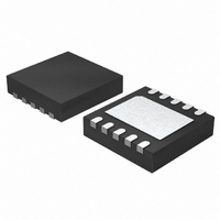
LTC2919IDDB-5#TRMPBF Linear Technology, LTC2919IDDB-5#TRMPBF Datasheet - Page 15

LTC2919IDDB-5#TRMPBF
Manufacturer Part Number
LTC2919IDDB-5#TRMPBF
Description
IC MONITOR PREC 5V 10-DFN
Manufacturer
Linear Technology
Type
Multi-Voltage Supervisorr
Datasheet
1.LTC2919CMS-5PBF.pdf
(16 pages)
Specifications of LTC2919IDDB-5#TRMPBF
Number Of Voltages Monitored
3
Output
Open Drain or Open Collector
Reset
Active Low
Reset Timeout
140 ms Minimum
Voltage - Threshold
4.425V, Adj, Adj
Operating Temperature
-40°C ~ 85°C
Mounting Type
Surface Mount
Package / Case
10-DFN
Lead Free Status / RoHS Status
Lead free / RoHS Compliant
Available stocks
Company
Part Number
Manufacturer
Quantity
Price
PACKAGE DESCRIPTIO
2.55 ±0.05
GAUGE PLANE
NOTE:
1. DRAWING CONFORMS TO VERSION (WECD-1) IN JEDEC PACKAGE OUTLINE M0-229
2. DRAWING NOT TO SCALE
3. ALL DIMENSIONS ARE IN MILLIMETERS
4. DIMENSIONS OF EXPOSED PAD ON BOTTOM OF PACKAGE DO NOT INCLUDE
5. EXPOSED PAD SHALL BE SOLDER PLATED
6. SHADED AREA IS ONLY A REFERENCE FOR PIN 1 LOCATION ON THE TOP AND BOTTOM OF PACKAGE
RECOMMENDED SOLDER PAD PITCH AND DIMENSIONS
NOTE:
1. DIMENSIONS IN MILLIMETER/(INCH)
2. DRAWING NOT TO SCALE
3. DIMENSION DOES NOT INCLUDE MOLD FLASH, PROTRUSIONS OR GATE BURRS.
4. DIMENSION DOES NOT INCLUDE INTERLEAD FLASH OR PROTRUSIONS.
5. LEAD COPLANARITY (BOTTOM OF LEADS AFTER FORMING) SHALL BE 0.102mm (.004") MAX
(.007)
1.15 ±0.05
0.18
MOLD FLASH. MOLD FLASH, IF PRESENT, SHALL NOT EXCEED 0.15mm ON ANY SIDE
MOLD FLASH, PROTRUSIONS OR GATE BURRS SHALL NOT EXCEED 0.152mm (.006") PER SIDE
INTERLEAD FLASH OR PROTRUSIONS SHALL NOT EXCEED 0.152mm (.006") PER SIDE
0.25 ± 0.05
0.64 ±0.05
(2 SIDES)
(.010)
0.254
2.39 ±0.05
(2 SIDES)
DETAIL “A”
DETAIL “A”
0.50 BSC
0° – 6° TYP
Information furnished by Linear Technology Corporation is believed to be accurate and reliable.
However, no responsibility is assumed for its use. Linear Technology Corporation makes no represen-
tation that the interconnection of its circuits as described herein will not infringe on existing patent rights.
(.021 ± .006)
0.53 ± 0.152
0.70 ±0.05
PACKAGE
OUTLINE
SEATING
U
PLANE
(Reference LTC DWG # 05-08-1722 Rev Ø)
(Reference LTC DWG # 05-08-1661 Rev E)
10-Lead Plastic DFN (3mm × 2mm)
3.00 ± 0.102
(.118 ± .004)
(SEE NOTE 6)
(.007 – .011)
(.193 ± .006)
4.90 ± 0.152
0.17 – 0.27
(NOTE 3)
TOP MARK
PIN 1 BAR
TYP
0.200 REF
10-Lead Plastic MSOP
(.043)
MAX
1.10
DDB Package
MS Package
(.0197)
0.50
BSC
10
1 2 3 4 5
9
3.00 ±0.10
(2 SIDES)
8
7 6
(.118 ± .004)
3.00 ± 0.102
(.0196 ± .003)
0.497 ± 0.076
(.034)
(NOTE 4)
0.86
REF
0.1016 ± 0.0508
MSOP (MS) 0307 REV E
(.004 ± .002)
2.00 ±0.10
0.75 ±0.05
REF
(2 SIDES)
0 – 0.05
(.0120 ± .0015)
0.305 ± 0.038
R = 0.05
0.64 ± 0.05
TYP
(2 SIDES)
TYP
(.206)
5.23
MIN
RECOMMENDED SOLDER PAD LAYOUT
0.25 ± 0.05
R = 0.115
BOTTOM VIEW—EXPOSED PAD
TYP
6
5
2.39 ±0.05
(2 SIDES)
LTC2919
10
1
0.889 ± 0.127
0.50 BSC
(.035 ± .005)
(.126 – .136)
3.20 – 3.45
0.40 ± 0.10
(.0197)
0.50
BSC
PIN 1
R = 0.20 OR
0.25 × 45°
CHAMFER
15
(DDB10) DFN 0905 REV Ø
2919f


