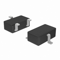
XC61CN2702MR-G Torex Semiconductor Ltd, XC61CN2702MR-G Datasheet

XC61CN2702MR-G
Specifications of XC61CN2702MR-G
Related parts for XC61CN2702MR-G
XC61CN2702MR-G Summary of contents
Page 1
XC61C Series Low Voltage Detectors (V Standard Voltage Detectors (V ■GENERAL DESCRIPTION The XC61C series are highly precise, low power consumption voltage detectors, manufactured using CMOS and laser trimming technologies. Detect voltage is extremely accurate with minimal temperature drift. Both ...
Page 2
XC61C Series ■PIN CONFIGURATION ■PIN ASSIGNMENT PIN NUMBER SSOT-24 SOT-23 SOT- ■PRODUCT CLASSIFICATION ●Ordering Information *1 XC61C①②③④⑤⑥⑦-⑧ DESIGNATOR ITEM Output Configuration ① Detect Voltage ②③ ④ Output Delay Detect Accuracy ...
Page 3
DIAGRAMS (1) CMOS Output ■ABSOLUTE MAXIMUM RATINGS PARAMETER Input Voltage Output Current CMOS Output Voltage N-ch Open Drain Output *1 N-ch Open Drain Output *2 SSOT-24 SOT-23 Power Dissipation SOT-89 TO-92 Operating Temperature Range Storage Temperature Range *1: Low ...
Page 4
XC61C Series ■ELECTRICAL CHARACTERISTICS V = 0.8V to 6.0V ± ( 2.6V to 5.1V ± (T) PARAMETER SYMBOL Detect Voltage V DF Hysteresis Range V HYS Supply Current I SS Operating Voltage *1 V ...
Page 5
EXPLANATION (Especially prepared for CMOS output products) ① When input voltage ( higher than detect voltage ( condition of high impedance exists with N-ch open drain output configurations.) ② When input voltage (V ) falls ...
Page 6
XC61C Series ■NOTES ON USE 1. Please use this IC within the stated absolute maximum ratings. For temporary, transitional voltage drop or voltage rising phenomenon, the IC is liable to malfunction should the ratings be exceeded. 2. When a resistor ...
Page 7
XC61C Series 7/18 ...
Page 8
XC61C Series ■TYPICAL PERFORMANCE CHARACTERISTICS ●Low Voltage Note : Unless otherwise stated, the N-ch open drain pull-up resistance value is 100kΩ. 8/18 ...
Page 9
PERFORMANCE CHARACTERISTICS (Continued) ●Low Voltage (Continued) (4) N-ch Driver Output Current vs. V XC61CC0902 (0.9V) 1.4 Ta=25℃ 1.2 V =0.8V IN 1.0 0.8 0.6 0.7V 0.4 0 0.2 0.4 0.6 0.8 V (V) DS XC61CC1502(1.5V) 1.4 Ta=25℃ ...
Page 10
XC61C Series ■TYPICAL PERFORMANCE CHARACTERISTICS (Continued) ●Standard Voltage (1) Supply Current vs. Input Voltage XC61CC1802 (1.8V) 3.5 3.0 2.5 2.0 Ta=85℃ 25℃ 1.5 1.0 -40℃ 0 Input Voltage: V (V) IN XC61CC3602 (3.6V) 3.5 ...
Page 11
PERFORMANCE CHARACTERISTICS (Continued) ●Standard Voltage (Continued) (3) Output Voltage vs. Input Voltage XC61CN1802 (1.8V) 2 Ta=25℃ Input Voltage: V (V) IN XC61CN3602 (3.6V) 4 Ta=25℃ Input Voltage: ...
Page 12
XC61C Series ■TYPICAL PERFORMANCE CHARACTERISTICS (Continued) ●Standard Voltage (Continued) (4) N-ch Driver Output Current vs. V XC61CC1802 (1.8V) 1000 V =0.8V Ta=25℃ IN 800 600 0.7V 400 200 0 0 0.2 0.4 0.6 0.8 V (V) DS XC61CC3602 (3.6V) 1000 ...
Page 13
PERFORMANCE CHARACTERISTICS (Continued) ●Standard Voltage (Continued) (6) P-ch Driver Output Current vs. Input Voltage XC61CC1802 (1.8 =2. Input Voltage: V (V) IN XC61CC3602 (3.6 =2.1V DS ...
Page 14
XC61C Series ■PACKAGING INFORMATION ●SSOT-24 2.0±0.1 +0.15 +0.15 0.25 -0.1 0.25 -0.1 +0.15 +0.15 0.25 -0.1 0.35 -0.1 0.05 1.3±0.2 ●SOT-89 14/18 ●SOT-23 +0 +0.1 0.125 -0.05 ...
Page 15
INFORMATION(Continued) ●TO-92 ●TB TYPE +0.35 4.65 -0.45 0.45±0.1 (1.27) ●TH TYPE 3.7±0.3 0.45±0.1 0.4±0.05 2.5 +0.35 4.65 -0.45 3.7±0.3 0.4±0.05 +0.4 +0.4 2.5 -0.1 -0.1 XC61C Series 15/18 ...
Page 16
XC61C Series ■MARKING RULE ● SSOT-24, SOT-23, SOT- ① ② ④ ① ② ③ ④ 16/18 ① represents integer of detect voltage and CMOS Output (XC61CC series) MARK CONFIGURATION A ...
Page 17
RULE (Continued) ●TO-92 TO-92 (SIDE VIEW) ① represents output configuration OUTPUT MARK CONFIGURATION C CMOS N N-ch ②, ③ represents detect voltage (ex.) MARK VOLTAGE (V) ② ③ 3 5.0 ④ represents delay time MARK ...
Page 18
... Should you wish to use the products under conditions exceeding the specifications, please consult us or our representatives assume no responsibility for damage or loss due to abnormal use. 7. All rights reserved. No part of this datasheet may be copied or reproduced without the prior permission of TOREX SEMICONDUCTOR LTD. 18/18 ...


