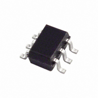
ADM1086AKSZ-REEL7 Analog Devices Inc, ADM1086AKSZ-REEL7 Datasheet - Page 13

ADM1086AKSZ-REEL7
Manufacturer Part Number
ADM1086AKSZ-REEL7
Description
IC SIMPLE SEQUENCER P-P SC70-6
Manufacturer
Analog Devices Inc
Type
Sequencerr
Datasheet
1.ADM1087AKSZ-REEL7.pdf
(16 pages)
Specifications of ADM1086AKSZ-REEL7
Number Of Voltages Monitored
1
Output
Push-Pull, Totem Pole
Reset
Active High
Reset Timeout
Adjustable/Selectable
Voltage - Threshold
Adjustable/Selectable
Operating Temperature
-40°C ~ 85°C
Mounting Type
Surface Mount
Package / Case
SC-70-6, SC-88, SOT-363
Threshold Voltage
0.6V
No. Of Supervisors / Monitors
1
Supply Voltage Range
2.25V To 3.6V
Reset Type
Active-High
Supply Current
15µA
Digital Ic Case Style
SC-70
No. Of Pins
6
Number Of Voltage Supervisors
1
Monitored Supervisor Voltage
0.6
Reset Threshold Voltage (min)
560mV
Reset Threshold Voltage (max)
640mV
Operating Supply Voltage (min)
2.25V
Operating Supply Voltage (max)
3.6V
Package Type
SC-70
Operating Temperature Classification
Automotive
Operating Temp Range
-40C to 125C
Pin Count
6
Mounting
Surface Mount
Lead Free Status / RoHS Status
Lead free / RoHS Compliant
Lead Free Status / RoHS Status
Lead free / RoHS Compliant, Lead free / RoHS Compliant
Other names
ADM1086AKSZ-REEL7
ADM1086AKSZ-REEL7TR
ADM1086AKSZ-REEL7TR
Available stocks
Company
Part Number
Manufacturer
Quantity
Price
Part Number:
ADM1086AKSZ-REEL7
Manufacturer:
ADI/亚德诺
Quantity:
20 000
DUAL LOFO SEQUENCING
A power sequencing solution for a portable device, such as a
PDA, is shown in Figure 27. This solution requires that the
microprocessor power supply turn on before the LCD display
turns on, and that the LCD display power-down before the
microprocessor powers down. In other words, the last power
supply to turn on is the first one to turn off (LOFO).
An RC network connects the battery and the SD input of the
ADP3333 voltage regulator. This causes power-up and power-
down transients to appear at the SD input when the battery is
connected and disconnected. The 3.3 V microprocessor supply
turns on quickly on power-up and turns off slowly on power-
down. This is due to two factors: Capacitor C1 charges up to
9 V on power-up and charges down from 9 V on power-down,
and the SD pin has logic high and logic low input levels of 2 V
and 0.4 V.
For the display power sequencing, the ADM1085 is equipped
with Capacitor C2 to create the delay between the micro-
processor and display power turning on. When the system is
powered down, the ADM1085 turns off the display power
immediately, while the 3.3 V regulator waits for C1 to discharge
to 0.4 V before switching off.
9V
MICROPROCESSOR
POWER SWITCH
SYSTEM
DISPLAY
SYSTEM
POWER
POWER
POWER
Figure 27. Dual LOFO Power-Supply Sequencing
V
C1
2.5V
9V
0V
9V
0V
0V
5V
0V
V
ENIN
IN
ADM1086
C1
SD
3.3V
ENOUT
ADP3333
CEXT
9V
C2
2.5V
SD
ADP3333
MICROPROCESSOR
POWER
9V
5V
DISPLAY
POWER
Rev. A | Page 13 of 16
SIMULTANEOUS ENABLING
The enable output can drive multiple enable or shutdown
regulator inputs simultaneously.
POWER GOOD SIGNAL DELAYS
Sometimes sequencing is performed by asserting power good
signals when the voltage regulators are already on, rather than
sequencing the power supplies directly. In these scenarios, a
simple sequencer IC can provide variable delays so that
enabling separate circuit blocks can be staggered in time.
For example, in a notebook PC application, a dedicated
microcomputer asserts a power good signal for North Bridge™
and South Bridge™ ICs. The ADM1086 delays the South Bridge
signal, so that it is enabled after the North Bridge.
12V
ADM1085/ADM1086/ADM1087/ADM1088
CONTROL
ENABLE
Figure 28. Enabling a Pair of Regulators from a Single ADM1085
MICROCOMPUTER
SD
ADP3333
5V
IN
OUT
Figure 29. Power Good Delay
POWER_GOOD
V
ENIN
3.3V
IN
V
ENIN
ADM1085
IN
ADM1086
3.3V
V
3.3V
CC
ENOUT
CEXT
ENOUT
CEXT
3.3V
SD
SD
EN
EN
ADP3333
ADP3333
BRIDGE
BRIDGE
NORTH
SOUTH
12V
5V
IC
5V
IC
IN
IN
OUT
OUT
2.5V
1.8V


