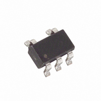
MAX6306UK30D1+T Maxim Integrated Products, MAX6306UK30D1+T Datasheet - Page 7

MAX6306UK30D1+T
Manufacturer Part Number
MAX6306UK30D1+T
Description
IC PROGRAM 3.000V RESET SOT23-5
Manufacturer
Maxim Integrated Products
Type
Multi-Voltage Supervisorr
Datasheet
1.MAX6309UK29D3T.pdf
(11 pages)
Specifications of MAX6306UK30D1+T
Number Of Voltages Monitored
2
Output
Open Drain or Open Collector
Reset
Active Low
Reset Timeout
1 ms Minimum
Voltage - Threshold
3V, Adj
Operating Temperature
0°C ~ 70°C
Mounting Type
Surface Mount
Package / Case
SOT-23-5, SC-74A, SOT-25
Monitored Voltage
3.3 V, 5 V
Undervoltage Threshold
2.955 V
Overvoltage Threshold
3.045 V
Output Type
Active Low, Open Drain
Manual Reset
Resettable
Watchdog
No Watchdog
Battery Backup Switching
No Backup
Power-up Reset Delay (typ)
1.4 ms
Supply Voltage (max)
5.5 V
Supply Voltage (min)
1 V
Supply Current (typ)
8 uA
Maximum Power Dissipation
571 mW
Maximum Operating Temperature
+ 70 C
Mounting Style
SMD/SMT
Minimum Operating Temperature
0 C
Power Fail Detection
No
Lead Free Status / RoHS Status
Lead free / RoHS Compliant
The ±25nA max input leakage current allows resistors on
the order of megohms. Choose the pull-up resistor in the
divider to minimize the error due to the input leakage cur-
rent. The error term in the calculated threshold is simply:
If you choose R1 to be 1MΩ, the resulting error is
±25 x 10
Like the V
MAX6309/MAX6310/MAX6312/MAX6313, the RST IN_
inputs (when used with a voltage divider) are designed to
ignore fast voltage transients. Increase the noise immunity
by connecting a capacitor on the order of 0.1µF between
RST IN and GND (Figure 2). This creates a single-pole
lowpass filter with a corner frequency given by:
For example, if R1 = 1MΩ and R2 = 1.6MΩ, adding a
0.1µF capacitor from RST IN_ to ground results in a
lowpass corner frequency of f = 2.59Hz. Note that
adding capacitance to RST IN slows the circuit’s overall
response time.
Since the RESET output on the MAX6305/MAX6306/
MAX6307 is open drain, these devices interface easily
with µPs that have bidirectional reset pins, such as the
Motorola 68HC11. Connecting the µP supervisor’s
RESET output directly to the microcontroller’s RESET
pin with a single pull-up resistor allows either device to
assert reset (Figure 3).
Figure 2. Increasing Noise Immunity
*FOR ADDITIONAL NOISE IMMUNITY
__________Applications Information
R1
R2
V
IN
-9
CC
x 1 x 10
f = (1/2π) / (R1 + R2)(R1 x R2 x C)
C*
voltage monitors on the MAX6306/MAX6307/
RST IN_
_ _ _ _ _ _ _ _ _ _ _ _ _ _ _ _ _ _ _ _ _ _ _ _ _ _ _ _ _ _ _ _ _ _ _ _ _ _ _ _ _ _ _ _ _ _ _ _ _ _ _ _ _ _ _ _ _ _ _ _ _ _ _ _ _ _ _ _ _ _ _ _ _ _ _ _ _ _ _ _ _ _ _ _ _ _ _ _ _ _ _ _ _ _ _ _ _ _ _ _ _ _ _ _ _ _ _ _ _ _ _ _ _ _ _ _ _ _ _ _ _ _ _ _ _ _ _ _ _ _ _ _ _ _ _ _ _ _ _ _ _ _ _ _ _ _ _ _ _ _ _ _ _ _ _ _ _ _ _ _ _ _ _ _ _ _ _ _ _ _ _ _ _ _
MAX6305–
6
MAX6313
= ±25mV.
GND
V
CC
±25nA x R1
Bidirectional Reset Pins
Interfacing to µPs with
V
*ƒ
TH
C
=
=
( )
2π
1
R1 + R2
(
R2
R1
R1 + R2
x
R2
V
x
RSTH
C
)
Programmable Reset ICs
In addition to issuing a reset to the µP during power-up,
power-down, and brownout conditions, these devices
are relatively immune to short-duration, negative-going
V
The Typical Operating Characteristics show the
Maximum Transient Duration vs. V
Overdrive, for which reset pulses are not generated.
The graph was produced using negative-going pulses,
starting at V
grammed reset threshold by the magnitude indicated
(reset threshold overdrive). The graph shows the maxi-
mum pulse width that a negative-going V
may typically have without causing a reset pulse to be
issued. As the amplitude of the transient increases (i.e.,
goes farther below the reset threshold), the maximum
allowable pulse width decreases.
RST IN_/OVRST IN are also immune to negative/positive-
going transients (see Typical Operating Characteristics ).
A 0.1µF bypass capacitor mounted close to the RST IN_,
OVRST IN, and/or the V
sient immunity.
When V
RESET current sinking (or sourcing) capabilities
decrease drastically. High-impedance CMOS-logic
inputs connected to RESET can drift to undetermined
voltages. This presents no problem in most applica-
tions, since most µPs and other circuitry do not operate
with V
must be valid down to 0V, adding a pull-down resistor
between RESET and ground sinks any stray leakage
Figure 3. Interfacing to µPs with Bidirectional Reset I/O
CC
transients (glitches).
5-Pin, Multiple-Input,
CC
GENERATOR
CC
RESET
below 1V. In those applications where RESET
MAX6305
MAX6306
MAX6307
falls below 1V, push/pull structured RESET/
GND
V
CC
TH
Negative-Going V
Ensuring a Valid RESET /RESET
max, and ending below the pro-
RESET
Output Down to V
CC
pin provides additional tran-
CC
CC
RESET
Reset Threshold
GND
V
Transients
μ
CC
P
CC
CC
transient
= 0V
7


