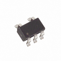
MAX6458UKD0C+T Maxim Integrated Products, MAX6458UKD0C+T Datasheet - Page 8

MAX6458UKD0C+T
Manufacturer Part Number
MAX6458UKD0C+T
Description
IC SUPPLY VOLT MONITR SOT23-5
Manufacturer
Maxim Integrated Products
Type
Simple Reset/Power-On Resetr
Datasheet
1.MAX6457UKD3CT.pdf
(15 pages)
Specifications of MAX6458UKD0C+T
Number Of Voltages Monitored
1
Output
Open Drain or Open Collector
Reset
Active Low
Reset Timeout
50 µs Typical
Voltage - Threshold
Adjustable/Selectable
Operating Temperature
-40°C ~ 125°C
Mounting Type
Surface Mount
Package / Case
SOT-23-5, SC-74A, SOT-25
Lead Free Status / RoHS Status
Lead free / RoHS Compliant
Each of the MAX6457–MAX6460 high-voltage (4V to
28V), low-power voltage monitors include a precision
bandgap reference, one or two low-offset-voltage com-
parators, internal threshold hysteresis, internal timeout
period, and one or two high-voltage open-drain outputs.
Two external resistors set the trip voltage, V
V
V
MAX6460’s high input impedance allows large-value
resistors without compromising trip-voltage accuracy.
To minimize current consumption, select a value for R2
between 10kΩ and 1MΩ, then calculate R1 as follows:
where V
threshold trip voltage (V
or V
Use the MAX6460 voltage reference (REF) to set the
trip threshold by connecting IN+ or IN- through a volt-
age divider (within the inputs common-mode voltage
range) to REF. Do not connect REF directly to IN+ or
IN- since this violates the input common-mode voltage
range. Small leakage currents into the comparators
inputs allows use of large value resistors to prevent
loading the reference and affecting its accuracy. Figure
5b shows an active-high power-good output. Use the
following equation to determine the resistor values
when connecting REF to IN-:
High-Voltage, Low-Current Voltage Monitors in
SOT Packages
Figure 5a. Programming the Trip Voltage
8
TRIP
CC
_______________________________________________________________________________________
TH
) toggles OUT. The MAX6457/MAX6458/MAX6459/
is the point at which the applied voltage (typically
Programming the Trip Voltage (V
- for undervoltage detection).
R1
R2
TRIP
V
CC
= desired trip voltage (in volts), V
R
IN+
GND
1
V
=
TRIP
R
2
Detailed Description
= V
MAX6457–
MAX6460
⎛
⎜
⎝
TH
TH
V
V
V
CC
TRIP
R1 + R2
TH
+ for overvoltage detection
(OUTA FOR
R2
MAX6459)
-
OUT
1
⎞
⎟
⎠
TRIP
R
PULLUP
OUT
(OUTA)
(Figure 5).
TRIP
TH
=
)
where V
V
old in (in volts).
For an active-low power-good output, connect the
resistor divider R1 and R2 to the inverting input and the
reference-divider network to the noninverting input.
Alternatively, connect an external reference less than
1.4V to either input.
Figure 5b. Programming the MAX6460 Trip Voltage
Figure 6. Input and Output Waveforms (Noninverting Input Varied)
REFD
V
V
IN+
OUT
V
V
V
R1
R2
TH+
CC
TH-
0
V
= divided reference, V
TRIP
REF
V
HYST
V
REFD
R3
R4
= reference output voltage (2.25V, typ),
V
R
REFD
1
=
R
t
TP
2
=
IN+
REF
IN-
⎛
⎜
⎝
V
V
REF
V
REFD
TRIP
MAX6460
⎛
⎜
⎝
GND
V
R
TRIP
CC
−
3
R
1
+
4
⎞
⎟
⎠
R
= desired trip thresh-
4
OUT
⎞
⎟
⎠
R
PULLUP
OUT
t
TP


