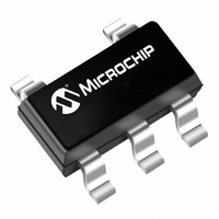
MCP1824T-1802E/OT Microchip Technology, MCP1824T-1802E/OT Datasheet - Page 17

MCP1824T-1802E/OT
Manufacturer Part Number
MCP1824T-1802E/OT
Description
IC LDO REG 300MA 1.8V SOT23-5
Manufacturer
Microchip Technology
Datasheet
1.MCP1824T-1802EOT.pdf
(34 pages)
Specifications of MCP1824T-1802E/OT
Regulator Topology
Positive Fixed
Voltage - Output
1.8V
Voltage - Input
2.1 ~ 6 V
Voltage - Dropout (typical)
0.2V @ 300mA
Number Of Regulators
1
Current - Output
300mA (Min)
Operating Temperature
-40°C ~ 125°C
Mounting Type
Surface Mount
Package / Case
SOT-23-5, SC-74A, SOT-25
Primary Input Voltage
2.12V
Output Voltage
1.8V
Dropout Voltage Vdo
200mV
No. Of Pins
5
Output Current
300mA
Voltage Regulator Case Style
SOT-23
Operating Temperature Range
-40°C To +125°C
Output Voltage Fixed
1.8V
Rohs Compliant
Yes
Number Of Outputs
1
Polarity
Positive
Input Voltage Max
6 V
Output Type
Fixed
Dropout Voltage (max)
0.32 V at 300 mA
Line Regulation
0.05 % / V
Load Regulation
0.5 %
Voltage Regulation Accuracy
2.5 %
Maximum Operating Temperature
+ 125 C
Mounting Style
SMD/SMT
Minimum Operating Temperature
- 40 C
Lead Free Status / RoHS Status
Lead free / RoHS Compliant
Current - Limit (min)
-
Lead Free Status / Rohs Status
Details
Other names
MCP1824T-1802E/OTTR
Available stocks
Company
Part Number
Manufacturer
Quantity
Price
Part Number:
MCP1824T-1802E/OT
Manufacturer:
MICROCHIP/微芯
Quantity:
20 000
3.0
The descriptions of the pins are listed in
TABLE 3-1:
3.1
The SHDN input is used to turn the LDO output voltage
on and off. When the SHDN input is at a logic-high
level, the LDO output voltage is enabled. When the
SHDN input is pulled to a logic-low level, the LDO
output voltage is disabled. When the SHDN input is
pulled low, the PWRGD output also goes low and the
LDO enters a low quiescent current shutdown state
where the typical quiescent current is 0.1 µA.
3.2
Connect the unregulated or regulated input voltage
source to V
several inches away from the LDO, or the input source
is a battery, it is recommended that an input capacitor
be used. A typical input capacitance value of 1 µF to
10 µF should be sufficient for most applications. The
type of capacitor used can be ceramic, tantalum, or
aluminum electrolytic. The low ESR characteristics of
the ceramic capacitor will yield better noise and PSRR
performance at high frequency.
3.3
For the optimal Noise and Power Supply Rejection
Ratio (PSRR) performance, the GND pin of the LDO
should be tied to an electrically quiet circuit ground.
This will help the LDO power supply rejection ratio and
noise performance. The ground pin of the LDO only
conducts the ground current of the LDO, so a heavy
trace is not required.
switching or noisy inputs, tie the GND pin to the return
of the output capacitor. Ground planes help lower
inductance and voltage spikes caused by fast transient
load currents and are recommended for applications
that are subjected to fast load transients.
Exposed
2007 Microchip Technology Inc.
Fixed
3-Pin
Pad
—
—
—
1
2
3
PIN DESCRIPTION
Shutdown Control Input (SHDN)
Input Voltage Supply (V
Ground (GND)
SOT-223
Exposed
IN
Fixed
5-Pin
. If the input voltage source is located
Pad
—
1
2
3
4
5
PIN FUNCTION TABLE
Exposed
5-Pin
Pad
Adj
—
For applications that have
1
2
3
4
5
Fixed
5-Pin
—
—
3
1
2
5
4
SOT-23
IN
Table
)
5-Pin
Adj
3-1.
—
—
3
1
2
5
4
PWRGD
SHDN
Name
V
GND
ADJ
V
EP
OUT
IN
MCP1824/MCP1824S
3.4
The V
LDO. A minimum output capacitance of 1.0 µF is
required for LDO stability. The MCP1824/MCP1824S is
stable
electrolytic capacitors. See Section 4.3 “Output
Capacitor” for output capacitor selection guidance.
3.5
For fixed applications, the PWRGD output is an open-
drain output used to indicate when the LDO output
voltage is within 92% (typically) of its nominal
regulation value. The PWRGD threshold has a typical
hysteresis value of 2%. The PWRGD output is delayed
by 110 µs (typical) from the time the LDO output is
within 92% + 3% (maximum hysteresis) of the
regulated output value on power-up. This delay time is
internally fixed.
3.6
For adjustable applications, the output voltage is
connected to the ADJ input through a resistor divider
that sets the output voltage regulation value. This
provides the users the capability to set the output
voltage to any value they desire within the 0.8V to 5.0V
range of the device.
3.7
The SOT-223 package has an exposed metal pad on
the bottom of the package. The exposed metal pad
gives the device better thermal characteristics by
providing a good thermal path to either the PCB or
heatsink to remove heat from the device. The exposed
pad of the package is at ground potential.
Description
Shutdown Control Input (active-low)
Input Voltage Supply
Ground
Regulated Output Voltage
Power Good Output
Output Voltage Adjust/Sense Input
Exposed Pad of the Package (ground potential)
OUT
with
Regulated Output Voltage (V
Power Good Output (PWRGD)
Output Voltage Adjust Input (ADJ)
Exposed Pad (EP)
pin is the regulated output voltage of the
ceramic,
tantalum,
DS22070A-page 17
and
aluminum-
OUT
)


