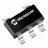
MCP1804T-5002I/OT Microchip Technology, MCP1804T-5002I/OT Datasheet - Page 5

MCP1804T-5002I/OT
Manufacturer Part Number
MCP1804T-5002I/OT
Description
IC REG LDO 5V 150MA SOT23-5
Manufacturer
Microchip Technology
Datasheet
1.MCP1804T-C002IOT.pdf
(38 pages)
Specifications of MCP1804T-5002I/OT
Package / Case
SOT-23-5, SC-74A, SOT-25
Regulator Topology
Positive Fixed
Voltage - Output
5V
Voltage - Input
Up to 28V
Voltage - Dropout (typical)
1V @ 100mA
Number Of Regulators
1
Current - Output
150mA (Min)
Operating Temperature
-40°C ~ 85°C
Mounting Type
Surface Mount
Input Voltage Max
28 V
Output Voltage
1.8 V
Output Voltage Tolerance
+/- 2 %
Dropout Voltage (max)
710 V
Output Current
150 mA
Line Regulation
0.05 %/V
Load Regulation
275 mV
Maximum Power Dissipation
250 mW
Maximum Operating Temperature
+ 85 C
Mounting Style
SMD/SMT
Minimum Operating Temperature
- 40 C
Primary Input Voltage
12V
Output Voltage Fixed
5V
Dropout Voltage Vdo
190mV
No. Of Pins
5
Operating Temperature Range
-40°C To +85°C
Voltage Regulator Type
LDO Linear
Rohs Compliant
Yes
Lead Free Status / RoHS Status
Lead free / RoHS Compliant
Current - Limit (min)
-
Lead Free Status / Rohs Status
Lead free / RoHS Compliant
Other names
MCP1804T-5002I/OTTR
Available stocks
Company
Part Number
Manufacturer
Quantity
Price
Part Number:
MCP1804T-5002I/OT
Manufacturer:
MICROCHIP/微芯
Quantity:
20 000
ELECTRICAL CHARACTERISTICS (CONTINUED)
TEMPERATURE SPECIFICATIONS
© 2009 Microchip Technology Inc.
Electrical Specifications: Unless otherwise specified, all limits are established for V
C
Power Supply Ripple
Rejection Ratio
Thermal Shutdown
Protection
Thermal Shutdown
Hysteresis
Note 1:
Temperature Ranges
Operating Temperature Range
Storage Temperature Range
Thermal Package Resistance
Thermal Resistance, 5LD SOT-23
Thermal Resistance, 3LD SOT-89
Thermal Resistance,
Thermal Resistance, 3LD SOT-223
OUT
Parameters
= 1 µF (X7R), C
2:
3:
4:
5:
The minimum V
V
For example: V
TCV
over the temperature range. V
Load regulation is measured at a constant junction temperature using low duty cycle pulse testing.
Changes in output voltage due to heating effects are determined using thermal regulation specification
TCV
Dropout voltage is defined as the input to output differential at which the output voltage drops 2% below its
measured value with an applied input voltage of V
R
Parameters
is the nominal regulator output voltage with an input voltage of V
OUT
OUT
.
= (V
5LD SOT-89
IN
OUT-HIGH
= 1 µF (X7R), V
R
IN
= 1.8V, 2.5V, 3.0V, 3.3V, etc.
PSRR
ΔTSD
must meet one condition: V
Sym
TSD
- V
OUT-LOW
SHDN
Sym
Tstg
OUT-LOW
θ
θ
θ
θ
θ
θ
T
JC
JC
JC
JA
JA
JA
A
Min
—
—
—
) *10
= V
IN
6
= lowest voltage measured over the temperature range.
Min
-40
-55
, T
/ (V
—
—
—
—
—
—
A
Typ
150
50
25
R
= +25°C
IN
* ΔTemperature), V
Typ
256
180
100
≥ (V
81
62
15
R
+ 2.0V.
R
Max
—
—
—
+ 2.0V).
+125
Max
+85
—
—
—
—
—
—
Units
Units
°C/W
°C/W
°C/W
OUT-HIGH
dB
°C
°C
°C
°C
IN
= V
EIA/JEDEC JESD51-7
FR-4 0.063 4-Layer Board
EIA/JEDEC JESD51-7
FR-4 0.063 4-Layer Board
EIA/JEDEC JESD51-7
FR-4 0.063 4-Layer Board
V
T
f = 1 kHz, I
IN
R
= highest voltage measured
INAC
J
+ 2.0V.
= V
R
= 0.5V pk-pk, C
MCP1804
+ 2.0V, Note 1,
Conditions
Conditions
L
= 20 mA,
DS22200B-page 5
IN
= 0 µF


