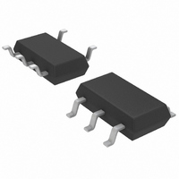
LT1761ES5-5#TRMPBF Linear Technology, LT1761ES5-5#TRMPBF Datasheet - Page 18

LT1761ES5-5#TRMPBF
Manufacturer Part Number
LT1761ES5-5#TRMPBF
Description
IC LDO REG 100MA 5V TSOT23-5
Manufacturer
Linear Technology
Specifications of LT1761ES5-5#TRMPBF
Regulator Topology
Positive Fixed
Voltage - Output
5V
Voltage - Input
Up to 20V
Voltage - Dropout (typical)
0.3V @ 100mA
Number Of Regulators
1
Current - Output
100mA
Current - Limit (min)
110mA
Operating Temperature
-40°C ~ 125°C
Mounting Type
Surface Mount
Package / Case
TSOT-23-5, TSOT-5, TSOP-5
Primary Input Voltage
6V
Output Voltage Fixed
5V
Dropout Voltage Vdo
300mV
No. Of Pins
5
Output Current
100mA
Voltage Regulator Case Style
SOT-23
Operating Temperature Range
-40°C To +125°C
Rohs Compliant
Yes
Lead Free Status / RoHS Status
Lead free / RoHS Compliant
Other names
LT1761ES5-5#PBF
LT1761ES5-5#PBF
LT1761ES5-5#TRMPBF
LT1761ES5-5#TRMPBFTR
LT1761ES5-5#PBF
LT1761ES5-5#TRMPBF
LT1761ES5-5#TRMPBFTR
Available stocks
Company
Part Number
Manufacturer
Quantity
Price
LT1761 Series
18
APPLICATIO S I FOR ATIO
from the 1.22V reference when the output is forced to 20V.
The top resistor of the resistor divider must be chosen to
limit the current into the ADJ pin to less than 5mA when the
ADJ pin is at 7V. The 13V difference between output and
ADJ pin divided by the 5mA maximum current into the ADJ
pin yields a minimum top resistor value of 2.6k.
In circuits where a backup battery is required, several
different input/output conditions can occur. The output
voltage may be held up while the input is either pulled to
ground, pulled to some intermediate voltage or is left open
U
U
W
100
90
80
70
60
50
40
30
20
10
Figure 6. Reverse Output Current
0
0
T
V
CURRENT FLOWS
INTO OUTPUT PIN
V
(LT1761-BYP, -SD)
U
J
IN
OUT
LT1761-3
= 25°C
LT1761-2.8
= 0V
1
= V
LT1761-2.5
2
ADJ
LT1761-2
LT1761-1.8
OUTPUT VOLTAGE (V)
LT1761-1.5
3
LT1761-1.2
4
LT1761-BYP
LT1761-SD
LT1761-5
5
circuit. Current flow back into the output will follow the
curve shown in Figure 6.
When the IN pin of the LT1761-X is forced below the OUT
pin or the OUT pin is pulled above the IN pin, input current
will typically drop to less than 2μA. This can happen if the
input of the device is connected to a discharged (low
voltage) battery and the output is held up by either a
backup battery or a second regulator circuit. The state of
the SHDN pin will have no effect on the reverse output
current when the output is pulled above the input.
6
7
LT1761-3.3
8
9
1761 F06
10
1761sfc


