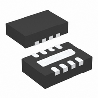
LT3020EDD#PBF Linear Technology, LT3020EDD#PBF Datasheet - Page 11

LT3020EDD#PBF
Manufacturer Part Number
LT3020EDD#PBF
Description
IC REG LDO ADJ 100MA LV 8-DFN
Manufacturer
Linear Technology
Datasheet
1.LT3020EDDPBF.pdf
(16 pages)
Specifications of LT3020EDD#PBF
Regulator Topology
Positive Adjustable
Voltage - Output
0.2 ~ 9.5 V
Voltage - Input
0.9 ~ 10 V
Voltage - Dropout (typical)
0.15V @ 100mA
Number Of Regulators
1
Current - Output
100mA
Current - Limit (min)
110mA
Operating Temperature
-40°C ~ 125°C
Mounting Type
Surface Mount
Package / Case
8-DFN
Lead Free Status / RoHS Status
Lead free / RoHS Compliant
Available stocks
Company
Part Number
Manufacturer
Quantity
Price
APPLICATIO S I FOR ATIO
response to light tapping from a pencil. Similar vibration
induced behavior can masquerade as increased output
voltage noise.
No-Load/Light-Load Recovery
A possible transient load step that occurs is where the
output current changes from its maximum level to zero
current or a very small load current. The output voltage
responds by overshooting until the regulator lowers the
amount of current it delivers to the new level. The regulator
loop response time and the amount of output capacitance
control the amount of overshoot. Once the regulator has
decreased its output current, the current provided by the
resistor divider (which sets V
remaining to discharge the output capacitor from the level
to which it overshot. The amount of time it takes for the
output voltage to recover easily extends to milliseconds
with microamperes of divider current and a few microfar-
ads of output capacitance.
To eliminate this problem, the LT3020 incorporates a
no-load or light-load recovery circuit. This circuit is a
voltage-controlled current sink that significantly improves
the light load transient response time by discharging the
output capacitor quickly and then turning off. The current
sink turns on when the output voltage exceeds 6% of the
nominal output voltage. The current sink level is then
proportional to the overdrive above the threshold up to a
maximum of approximately 15mA. Consult the curve in
the Typical Performance Characteristics for the No-Load
Recovery Threshold.
If external circuitry forces the output above the no load
recovery circuit’s threshold, the current sink turns on in an
attempt to restore the output voltage to nominal. The
current sink remains on until the external circuitry releases
the output. However, if the external circuitry pulls the
output voltage above the input voltage, or the input falls
below the output, the LT3020 turns the current sink off and
shuts down the bias current/reference generator circuitry.
Thermal Considerations
The LT3020’s power handling capability is limited by its
maximum rated junction temperature of 125°C. The power
dissipated by the device is comprised of two components:
U
U
OUT
W
) is the only current
U
1. Output current multiplied by the input-to-output volt-
2. GND pin current multiplied by the input voltage:
GND pin current is found by examining the GND pin
current curves in the Typical Performance Characteristics.
Power dissipation is equal to the sum of the two compo-
nents listed above.
The LT3020 regulator has internal thermal limiting (with
hysteresis) designed to protect the device during overload
conditions. For normal continuous conditions, do not
exceed the maximum junction temperature rating of 125°C.
Carefully consider all sources of thermal resistance from
junction to ambient including other heat sources mounted
in proximity to the LT3020.
The underside of the LT3020 DD package has exposed metal
(4mm
This allows heat to directly transfer from the die junction
to the printed circuit board metal to control maximum
operating junction temperature. The dual-in-line pin ar-
rangement allows metal to extend beyond the ends of the
package on the topside (component side) of a PCB. Con-
nect this metal to GND on the PCB. The multiple IN and OUT
pins of the LT3020 also assist in spreading heat to the PCB.
The LT3020 MS8 package has pin 4 fused with the lead
frame. This also allows heat to transfer from the die to the
printed circuit board metal, therefore reducing the thermal
resistance. Copper board stiffeners and plated through-
holes can also be used to spread the heat generated by
power devices.
The following tables list thermal resistance for several
different board sizes and copper areas for two different
packages. Measurements were taken in still air on 3/32"
FR-4 board with one ounce copper.
Table 1. Measured Thermal Resistance for DD Package
TOPSIDE*
2500mm
900mm
225mm
100mm
age differential: (I
(I
50mm
GND
COPPER AREA
2
) from the lead frame to where the die is attached.
2
)(V
2
2
2
2
IN
BACKSIDE
).
2500mm
2500mm
2500mm
2500mm
2500mm
LT3020-1.5/LT3020-1.8
2
2
2
2
2
OUT
LT3020/LT3020-1.2/
BOARD AREA (JUNCTION-TO-AMBIENT)
)(V
2500mm
2500mm
2500mm
2500mm
2500mm
IN
– V
2
2
2
2
2
OUT
) and
THERMAL RESISTANCE
35°C/W
40°C/W
55°C/W
60°C/W
70°C/W
11
3020fc


