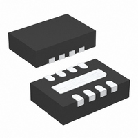
LT1965EDD-2.5#PBF Linear Technology, LT1965EDD-2.5#PBF Datasheet - Page 5

LT1965EDD-2.5#PBF
Manufacturer Part Number
LT1965EDD-2.5#PBF
Description
IC REG LDO 2.5V 1.1A 8-DFN
Manufacturer
Linear Technology
Datasheet
1.LT1965EDD-3.3PBF.pdf
(20 pages)
Specifications of LT1965EDD-2.5#PBF
Regulator Topology
Positive Fixed
Voltage - Output
2.5V
Voltage - Input
Up to 20V
Voltage - Dropout (typical)
0.31V @ 1.1A
Number Of Regulators
1
Current - Output
1.1A
Current - Limit (min)
1.2A
Operating Temperature
-40°C ~ 125°C
Mounting Type
Surface Mount
Package / Case
8-DFN
Lead Free Status / RoHS Status
Lead free / RoHS Compliant
Available stocks
Company
Part Number
Manufacturer
Quantity
Price
ELECTRICAL CHARACTERISTICS
temperature range, otherwise specifi cations are at T
PARAMETER
Current Limit
Input Reverse Leakage Current
Reverse Output Current (Note 11)
Note 1: Stresses beyond those listed under Absolute Maximum Ratings
may cause permanent damage to the device. Exposure to any Absolute
Maximum Rating condition for extended periods may affect device
reliability and lifetime.
Note 2: Absolute maximum input to output differential voltage is not
achievable with all combinations of rated IN pin and OUT pin voltages.
With the IN pin at 22V, the OUT pin may not be pulled below 0V. The total
measured voltage from IN to OUT must not exceed ±22V.
Note 3: The LT1965 regulators are tested and specifi ed under pulse load
conditions such that T
at T
characterization, and correlation with statistical process controls. The
LT1965I regulators are guaranteed over the full –40°C to 125°C operating
junction temperature range.
Note 4: The LT1965 adjustable version is tested and specifi ed for these
conditions with the ADJ connected to the OUT pin.
Note 5: Maximum junction temperature limits operating conditions. The
regulated output voltage specifi cation does not apply for all possible
combinations of input voltage and output current. Limit the output current
range if operating at the maximum input voltage. Limit the input-to-output
voltage differential if operating at the maximum output current.
Note 6: To satisfy minimum input voltage requirements, the LT1965
adjustable version is tested and specifi ed for these conditions with an
external resistor divider (bottom 4.02k, top 4.32k) for an output voltage of
A
= 25°C. Performance at –40°C and 125°C is assured by design,
J
≅ T
A
. The LT1965E regulators are 100% tested
CONDITIONS
V
V
V
LT1965-1.5, V
LT1965-1.8, V
LT1965-2.5, V
LT1965-3.3, V
LT1965 (Note 4), V
IN
IN
IN
= 7V, V
= V
= –20V, V
OUT(NOMINAL)
OUT
OUT
A
OUT
OUT
OUT
OUT
= 0
= 25°C. (Note 3)
= 0
= 1.5V, V
= 1.8V, V
= 2.5V, V
= 3.3V, V
OUT
+ 1V, ΔV
The
= 1.2V, V
l
IN
IN
IN
IN
denotes the specifi cations which apply over the full operating
OUT
= 0
= 0
= 0
= 0
IN
= -0.1V (Note 6)
2.5V. The external resistor divider adds 300μA of output DC load current.
This external current is not factored into GND pin current.
Note 7: Dropout voltage is the minimum input-to-output voltage
differential needed to maintain regulation at a specifi ed output current. In
dropout, the output voltage equals: (V
Note 8: GND pin current is tested with V
current source load. GND pin current increases slightly in dropout. For
the fi xed output versions, an internal resistor divider will typically add
100μA to the GND pin current. See GND pin current curves in the Typical
Performance Characteristics section.
Note 9: ADJ pin bias current fl ows into the ADJ pin.
Note 10: SHDN pin current fl ows into the SHDN pin.
Note 11: Reverse output current is tested with the IN pin grounded and the
OUT pin forced to the rated output voltage. This current fl ows into the OUT
pin and out of the GND pin.
Note 12: For the LT1965, LT1965-1.5 and LT1965-1.8, the minimum
input voltage specifi cation limits the dropout voltage under some output
voltage/load conditions.
Note 13: This IC includes overtemperature protection that is intended
to protect the device during momentary overload conditions. Junction
temperature will exceed 125°C when overtemperature is active.
Continuous operation above the specifi ed maximum operating junction
temperature may impair device reliability.
= 0
l
MIN
1.2
IN
LT1965 Series
– V
IN
= V
DROPOUT
OUT(NOMINAL)
TYP
275
275
275
275
175
2.4
)
MAX
525
525
525
525
400
1
+ 1V and a
UNITS
1965fa
5
mA
μA
μA
μA
μA
μA
A
A


