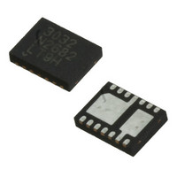
LT3032IDE#PBF Linear Technology, LT3032IDE#PBF Datasheet

LT3032IDE#PBF
Specifications of LT3032IDE#PBF
Available stocks
Related parts for LT3032IDE#PBF
LT3032IDE#PBF Summary of contents
Page 1
... DFN package with exposed back- side pads for each regulator, allowing optimum thermal performance. L, LT, LTC, LTM, Linear Technology and the Linear logo are registered trademarks and ThinSOT is a trademark of Linear Technology Corporation. All other trademarks are the property of their respective owners. 5V OUT AT 150mA 20µV ...
Page 2
... Output Short-Circuit Duration .......................... Indefinite Operating Junction Temperature Range (Note Grades ............................................. –40°C to 125°C Storage Temperature Range .................. –65°C to 150°C orDer inForMaTion LEAD FREE FINISH TAPE AND REEL LT3032EDE#PBF LT3032EDE#TRPBF LT3032IDE#PBF LT3032IDE#TRPBF LT3032EDE-5#PBF LT3032EDE-5#TRPBF LT3032IDE-5#PBF LT3032IDE-5#TRPBF LEAD BASED FINISH TAPE AND REEL LT3032EDE ...
Page 3
T PARAMETER Minimum INP Operating Voltage Minimum INN Operating Voltage Regulated Output Voltage LT3032-5 V (Notes 4, 10) LT3032-5 V ADJP Pin Voltage LT3032 (Notes 4, 5) ADJN Pin Voltage LT3032 (Notes ...
Page 4
LT3032 Series elecTrical characTerisTics temperature range, otherwise specifications are at T PARAMETER SHDNP Pin Current (Note 9) SHDNN Pin Current (Note 9) Quiescent Current in Shutdown Output Voltage Noise (10Hz to 100kHz) Ripple Rejection 120Hz ...
Page 5
Typical perForMance characTerisTics INP-to-OUTP Typical Dropout Voltage 500 450 400 350 T = 125°C J 300 250 200 T = 25°C J 150 100 100 120 140 160 LOAD CURRENT (mA) 3032 G01 ...
Page 6
LT3032 Series Typical perForMance characTerisTics LT3032 ADJN Pin Voltage –1.240 I = –1mA L –1.235 –1.230 –1.225 –1.220 –1.215 –1.210 –1.205 –1.200 –50 – 100 TEMPERATURE (°C) 3032 G08 LT3032 INP Quiescent Current ...
Page 7
Typical perForMance characTerisTics LT3032 Negative Side GND Pin Current –3 25° SHDNN INN *FOR V = –1.22V OUTN –2 8. –150mA* L –2 12 ...
Page 8
LT3032 Series Typical perForMance characTerisTics SHDNN Pin Input Current –15V INN POSITIVE CURRENT 9 FLOWS INTO THE PIN 15V SHDNN –15V SHDNN –3 –6 –9 –50 – ...
Page 9
Typical perForMance characTerisTics Reverse OUTP Pin Current INP V = 1.22V OUTP – 100 –25 TEMPERATURE (°C) 3032 G28 INN-to-OUTN Ripple Rejection –150mA ...
Page 10
LT3032 Series Typical perForMance characTerisTics Positive Load Regulation 0 –2 LT3032 –4 –6 –8 LT3032-5 –10 –12 –14 – +1V INP OUTP(NOMINAL) –18 ∆I = 1mA TO 150mA L –20 –50 – 100 ...
Page 11
Typical perForMance characTerisTics OUTP 10Hz to 100kHz Output Noise BYPP V OUTP 100µV/DIV 3032 G44 C = 10µF 1ms/DIV OUTP I = 150mA OUTP OUTN, 10Hz to 100kHz Output Noise 0.01µF ...
Page 12
LT3032 Series pin FuncTions OUTP (Pin 1): Positive Output. This output supplies power to the positive side load. A minimum output capacitor of 2.2µF is required to prevent oscillations. Larger out- put capacitors are required for applications with large transient ...
Page 13
FuncTions BYPN (Pin 11): Negative Bypass. The BYPN pin is used to bypass the reference of the negative side regulator to achieve low noise performance. A small capacitor from OUTN to this pin will bypass the reference to lower ...
Page 14
LT3032 Series applicaTions inForMaTion The LT3032 is a dual 150mA positive and negative low noise low dropout linear regulator with micropower quiescent current and shutdown. It supplies ±150mA at a dropout of 300mV. Output voltage noise can be lowered on ...
Page 15
BYPN pin operates at approximately –60mV. DC leakages on the order of 1µA into or out of these pins can throw off the internal reference by 20% or more. Output Capacitance ...
Page 16
LT3032 Series applicaTions inForMaTion 20 BOTH CAPACITORS ARE 16V, 1210 CASE SIZE, 10µF 0 X5R –20 –40 –60 Y5V –80 –100 BIAS VOLTAGE (V) Figure 3. Ceramic Capacitor DC Bias Characteristics 40 20 ...
Page 17
If wiring modifications are not permissible for the applications, including series resistance between the power supply and the input of the LT3032 also stabilizes the application. As little as 0.1Ω to 0.5Ω, often less, is effective in damping ...
Page 18
LT3032 Series applicaTions inForMaTion Calculating Junction Temperature Example: Given a positive output voltage of 3.3V, a positive input voltage 6V, output current range from 10mA to 150mA, negative output voltage of –3.3V, negative input voltage of –5V ...
Page 19
In situations where the ADJP pin is connected to a resistor divider that would pull the ADJP pin above its 7V clamp voltage if the output is pulled high, the ADJP pin input current must be limited to ...
Page 20
LT3032 Series package DescripTion 1.78 ±0.05 0.10 TYP 3.50 ±0.05 0.51 TYP 1.65 ± 0.05 2.10 ±0.05 RECOMMENDED SOLDER PAD PITCH AND DIMENSIONS APPLY SOLDER MASK TO AREAS THAT ARE NOT SOLDERED 4.00 ±0.10 (2 SIDES) PIN 1 TOP MARK ...
Page 21
... Revised quiescent current for the positive side up to 25µA in Applications Information. Information furnished by Linear Technology Corporation is believed to be accurate and reliable. However, no responsibility is assumed for its use. Linear Technology Corporation makes no representa- tion that the interconnection of its circuits as described herein will not infringe on existing patent rights. ...
Page 22
... ISD < 1μA; DFN and MS10E Q = 60μA, ISD < 1μA; DFN and Q = 50μA, ISD < 1μA; DFN and MS10E Q = 60μA, ISD < 1μA; DFN and Q LT 0111 REV B • PRINTED IN USA LINEAR TECHNOLOGY CORPORA TION 2010 3032fb ...


