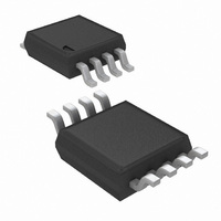
LP3982IMM-3.3/NOPB National Semiconductor, LP3982IMM-3.3/NOPB Datasheet - Page 3

LP3982IMM-3.3/NOPB
Manufacturer Part Number
LP3982IMM-3.3/NOPB
Description
IC REG LDO 300MA 3.3V 8MSOP
Manufacturer
National Semiconductor
Datasheet
1.LP3982IMMX-ADJ.pdf
(12 pages)
Specifications of LP3982IMM-3.3/NOPB
Regulator Topology
Positive Fixed
Voltage - Output
3.3V
Voltage - Input
Up to 6V
Voltage - Dropout (typical)
0.12V @ 300mA
Number Of Regulators
1
Current - Output
300mA (Min)
Current - Limit (min)
330mA
Operating Temperature
-40°C ~ 85°C
Mounting Type
Surface Mount
Package / Case
8-MSOP, Micro8™, 8-uMAX, 8-uSOP,
Voltage Regulator Type
Linear
Topology
LDO
Regulator Output Type
Fixed
Polarity Type
Positive
Number Of Outputs
Single
Input Voltage (min)
2.5V
Input Voltage (max)
6V
Output Voltage
3.3V
Package Type
MSOP
Output Current
300mA
Load Regulation
0.002%/mA
Line Regulation
0.01%/V
Output Voltage Accuracy
±2%
Operating Temp Range
-40C to 85C
Operating Temperature Classification
Industrial
Dropout Voltage@current (max)
0.22@200mA
Pin Count
8
Mounting
Surface Mount
Lead Free Status / RoHS Status
Lead free / RoHS Compliant
Other names
LP3982IMM-3.3
LP3982IMM-3.3TR
LP3982IMM-3.3TR
Available stocks
Company
Part Number
Manufacturer
Quantity
Price
Electrical Characteristics
Note 2: All voltages are with respect to the potential at the ground pin.
Note 3: Maximum Power dissipation for the device is calculated using the following equations:
where T
package θ
thus below 25˚C the power dissipation figure can be increased by 4.5mW per degree, and similarity decreased by this factor for temperatures above 25˚C. The value
of the θ
resistance and power dissipation for the LLP package, refer to Application Note AN-1187.
Note 4: Typical Values represent the most likely parametric norm.
Note 5: All limits are guaranteed by testing or statistical analysis.
Note 6: Human body model: 1.5kΩ in series with 100pF.
Note 7: Condition does not apply to input voltages below 2.5V since this is the minimum input operating voltage.
Note 8: Dropout voltage is measured by reducing V
version.
Note 9: The SET pin is not externally connected for the fixed versions.
Note 10: The FAULT detection voltage is specified for the input to output voltage differential at which the FAULT pin goes active low.
Functional Block Diagram
JA
J(MAX)
JA
for the LLP package is specifically dependent on the PCB trace area, trace material, and the number of layers and thermal vias. For improved thermal
= 223˚C/W, T
is the maximum junction temperature, T
J(MAX)
= 150˚C and using T
IN
A
until V
A
(Continued)
= 25˚C, the maximum power dissipation is found to be 561mW. The derating factor (−1/θ
is the ambient temperature, and θ
O
drops 100mV from its nominal value at V
3
JA
is the junction-to-ambient thermal resistance. E.g. for the MSOP-8
IN
-V
O
= 0.5V. Dropout Voltage does not apply to the 1.8
20036913
JA
) = −4.5mW/˚C,
www.national.com


