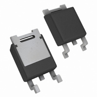
LM1117DT-ADJ/NOPB National Semiconductor, LM1117DT-ADJ/NOPB Datasheet - Page 7

LM1117DT-ADJ/NOPB
Manufacturer Part Number
LM1117DT-ADJ/NOPB
Description
IC REG LDO 800MA ADJ TO-252
Manufacturer
National Semiconductor
Type
Voltage Regulatorr
Specifications of LM1117DT-ADJ/NOPB
Regulator Topology
Positive Adjustable
Voltage - Output
1.25 ~ 13.8 V
Voltage - Input
2.65 ~ 15 V
Voltage - Dropout (typical)
1.2V @ 800mA
Number Of Regulators
1
Current - Output
800mA
Current - Limit (min)
800mA
Operating Temperature
0°C ~ 125°C
Mounting Type
Surface Mount
Package / Case
TO-252-2, DPak (2 Leads + Tab), TO-252AA, SC-63
Current, Output
800 mA
Current, Supply
5 mA
Package Type
TO-252
Regulation, Line
1 mV
Regulation, Load
1 mV
Regulator Type
DC-DC, Linear, Low Dropout
Resistance, Thermal, Junction To Case
10 °C/W
Temperature, Operating, Range
0 to +125 °C
Voltage, Dropout
1.2 V
Voltage, Input
15 V
Voltage, Noise
0.003 %
Voltage, Output
1.25 to 13.8 V
Voltage, Supply, Rejection Ratio
75 dB
Number Of Outputs
1
Polarity
Positive
Input Voltage Max
15 V
Output Voltage
1.25 V to 13.8 V
Output Type
Adjustable
Dropout Voltage (max)
1.2 V at 100 mA
Output Current
1.5 A
Line Regulation
0.035 %
Load Regulation
0.2 %
Voltage Regulation Accuracy
+/- 1 %
Maximum Operating Temperature
+ 125 C
Mounting Style
SMD/SMT
Minimum Operating Temperature
0 C
Reference Voltage
1.262 V
Lead Free Status / RoHS Status
Lead free / RoHS Compliant
Other names
*LM1117DT-ADJ
*LM1117DT-ADJ/NOPB
LM1117DT-ADJ
*LM1117DT-ADJ/NOPB
LM1117DT-ADJ
Available stocks
Company
Part Number
Manufacturer
Quantity
Price
, θ
Note 2: The maximum power dissipation is a function of T
, and T
. The maximum allowable power dissipation at any ambient temperature is
J(max)
JA
A
P
= (T
–T
)/θ
. All numbers apply for packages soldered directly into a PC board.
D
J(max)
A
JA
Note 3: For testing purposes, ESD was applied using human body model, 1.5kΩ in series with 100pF.
Note 4: Typical Values represent the most likely parametric norm.
Note 5: All limits are guaranteed by testing or statistical analysis.
Note 6: Load and line regulation are measured at constant junction room temperature.
Note 7: The dropout voltage is the input/output differential at which the circuit ceases to regulate against further reduction in input voltage. It is measured when the
output voltage has dropped 100mV from the nominal value obtained at V
= V
+1.5V.
IN
OUT
Note 8: The minimum output current required to maintain regulation.
2
Note 9: Minimum pad size of 0.038in
Note 10: Thermal Performance for the LLP was obtained using JESD51-7 board with six vias and an ambient temperature of 22˚C. For information about improved
thermal performance and power dissipation for the LLP, refer to Application Note AN-1187.
Typical Performance Characteristics
Dropout Voltage (V
-V
)
Short-Circuit Current
IN
OUT
10091922
10091923
Load Regulation
LM1117-ADJ Ripple Rejection
10091943
10091906
7
www.national.com


