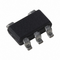
MIC5205-2.9YM5 TR Micrel Inc, MIC5205-2.9YM5 TR Datasheet - Page 8

MIC5205-2.9YM5 TR
Manufacturer Part Number
MIC5205-2.9YM5 TR
Description
IC REG LDO 150MA 1% 2.9V SOT23-5
Manufacturer
Micrel Inc
Datasheet
1.MIC5205-3.0YM5_TR.pdf
(10 pages)
Specifications of MIC5205-2.9YM5 TR
Regulator Topology
Positive Fixed
Voltage - Output
2.9V
Voltage - Input
Up to 16V
Voltage - Dropout (typical)
0.165V @ 150mA
Number Of Regulators
1
Current - Output
150mA
Operating Temperature
-40°C ~ 125°C
Mounting Type
Surface Mount
Package / Case
SOT-23-5, SC-74A, SOT-25
Lead Free Status / RoHS Status
Lead free / RoHS Compliant
Current - Limit (min)
-
Other names
576-2737-2
MIC5205-2.9YM5 TR
MIC5205-2.9YM5TR
MIC5205-2.9YM5TR
MIC5205-2.9YM5 TR
MIC5205-2.9YM5TR
MIC5205-2.9YM5TR
Application Information
Enable/Shutdown
Forcing EN (enable/shutdown) high (> 2V) enables the
regulator. EN is compatible with CMOS logic gates.
If the enable/shutdown feature is not required, connect
EN (pin 3) to IN (supply input, pin 1). See Figure 1.
Input Capacitor
A 1µF capacitor should be placed from IN to GND if
there is more than 10 inches of wire between the input
and the ac filter capacitor or if a battery is used as the
input.
Reference Bypass Capacitor
BYP (reference bypass) is connected to the internal
voltage reference. A 470pF capacitor (C
from BYP to GND quiets this reference, providing a
significant reduction in output noise. C
regulator phase margin; when using C
capacitors of 2.2µF or greater are generally required to
maintain stability.
The start-up speed of the MIC5205 is inversely
proportional to the size of the reference bypass
capacitor. Applications requiring a slow ramp-up of
output voltage should consider larger values of C
Likewise, if rapid turn-on is necessary, consider omitting
C
If output noise is not a major concern, omit C
leave BYP open.
Output Capacitor
An output capacitor is required between OUT and GND
to prevent oscillation. The minimum size of the output
capacitor is dependent upon whether a reference bypass
capacitor is used. 1.0µF minimum is recommended
when C
recommended when C
Larger
response. The output capacitor value may be increased
without limit.
The output capacitor should have an ESR (effective
series resistance) of about 5Ω or less and a resonant
frequency above 1MHz. Ultra-low-ESR capacitors can
cause a low amplitude oscillation on the output and/or
underdamped transient response. Most tantalum or
aluminum electrolytic capacitors are adequate; film types
will work, but are more expensive. Since many aluminum
electrolytics have electrolytes that freeze at about –
30°C, solid tantalums are recommended for operation
below –25°C.
At
capacitance is required for output stability. The capacitor
can be reduced to 0.47⎧F for current below 10mA or
Micrel
February 2006
BYP
.
lower
BYP
values
is not used (see Figure 2). 2.2µF minimum is
values
improve
of
BYP
output
is 470pF (see Figure 1).
the
current,
regulator’s
BYP
BYP
less
) connected
reduces the
BYP
, output
transient
BYP
output
and
BYP
.
8
0.33µF for currents below 1mA.
No-Load Stability
The MIC5205 will remain stable and in regulation with no
load (other than the internal voltage divider) unlike many
other voltage regulators. This is especially important in
CMOS RAM keep-alive applications.
Thermal Considerations
The MIC5205 is designed to provide 150mA of
continuous current in a very small package. Maximum
power dissipation can be calculated based on the output
current and the voltage drop across the part. To
determine the maximum power dissipation of the
package, use the junction-to-ambient thermal resistance
of the device and the following basic equation:
T
125°C, and T
is layout dependent; Table 1 shows examples of
junction-toambient thermal resistance for the MIC5205.
The actual power dissipation of the regulator circuit can
be determined using the equation:
Substituting P
conditions that are critical to the application will give the
maximum operating conditions for the regulator circuit.
For example, when operating the MIC5205-3.3BM5 at
room temperature with a minimum footprint layout, the
maximum input voltage for a set output current can be
determined as follows:
The junction-to-ambient thermal resistance for the
minimum footprint is 220°C/W, from Table 1. The
maximum power dissipation must not be exceeded for
proper operation. Using the output voltage of 3.3V and
an output current of 150mA, the maximum input voltage
can be determined. From the Electrical Characteristics
table, the maximum ground current for 150mA output
current is 2500µA or 2.5mA.
SOT-23-5(M5)
J(max)
Package
P
455mW = (V
455mW = V
950mW = V
P
P
P
D
D(max)
D(max)
D(max)
= (V
is the maximum junction temperature of the die,
Table 1. SOT-23-5 Thermal Resistance
IN
=
=
=
A
– V
D(max)
455mW
(
(
125
T
is the ambient operating temperature. θ
IN
IN
J(max)
Recommended
IN
OUT
×150mA – 495mW + V
×152.5mA
220
– 3.3V) 150mA + V
°
Minimum
Footprint
θ
220°C/W
C
) I
for P
JA
°
θJA
OUT
−
C/W
−
25
T
D
+ V
A
°
C
and solving for the operating
)
)
IN
I
GND
Copper Clad
θJA Square
170°C/W
IN
·2.5mA
IN
(408) 955-1690
·2.5mA
M9999-020806
MIC5205
130°C/W
θJC
JA


