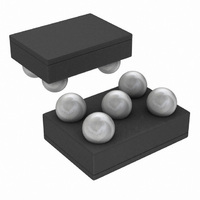
LP5952TL-1.2/NOPB National Semiconductor, LP5952TL-1.2/NOPB Datasheet - Page 5

LP5952TL-1.2/NOPB
Manufacturer Part Number
LP5952TL-1.2/NOPB
Description
IC REG LDO 1.2V 350MA MICRO5
Manufacturer
National Semiconductor
Series
PowerWise®r
Datasheet
1.LP5952TL-1.2EV.pdf
(16 pages)
Specifications of LP5952TL-1.2/NOPB
Regulator Topology
Positive Fixed
Voltage - Output
1.2V
Voltage - Input
Up to 4.5V
Voltage - Dropout (typical)
0.088V @ 350mA
Number Of Regulators
1
Current - Output
350mA
Operating Temperature
-40°C ~ 85°C
Mounting Type
Surface Mount
Package / Case
5-MicroSMD
For Use With
LP5952TL-1.2EV - BOARD EVALUATION LP5952TL-1.2
Lead Free Status / RoHS Status
Lead free / RoHS Compliant
Current - Limit (min)
-
Other names
LP5952TL-1.2
LP5952TL-1.2TR
LP5952TL-1.2TR
Available stocks
Company
Part Number
Manufacturer
Quantity
Price
Company:
Part Number:
LP5952TL-1.2/NOPB
Manufacturer:
Texas Instruments
Quantity:
10 000
Absolute Maximum Ratings
If Military/Aerospace specified devices are required,
please contact the National Semiconductor Sales Office/
Distributors for availability and specifications.
ESD Caution Notice
National Semiconductor recommends that all integrated circuits be handled with appropriate precautions. Failure to observe proper
ESD handling techniques can result in damage.
Electrical Characteristics
Typical values and limits appearing in standard typeface are for T
operating temperature range: -40°C
with V
V
V
V
V
EN pin, Voltage to GND:
Continuous Power Dissipation
(Note 3):
Junction Temperature (T
Storage Temperature Range:
Package Peak Reflow Temperature
(Pb-free, 10-20 sec.) (Note 4):
ESD Rating (Note 5):
Machine Model:
ΔV
ΔV
ΔV
ΔV
I
V
(Note 10)
V
E
SC
EN
IN
IN
BATT
DO_VBATT
DO_VIN
N
Human Body Model:
, V
OUT
OUT
OUT
OUT
≤
= V
Symbol
IN
BATT
V
pin to V
/ V
/ ΔV
/ ΔV
/ ΔmA
BATT
BATT
= V
OUT
pins: Voltage to GND,
OUT(NOM)
.
IN
BATT
:
IN
pin:
Output Voltage Tolerance
Line Regulation Error
Load Regulation Error
Output Current
(short circuit)
Output Voltage Dropout V
(Note 9)
Output Voltage Dropout V
Output Noise
+ 1.0V, V
J-MAX
Parameter
BATT
):
= V
≤
OUT(NOM)
T
J
≤
-65°C to + 150°C
Internally Limited
(Notes 2, 8, 11)
+125°C. Unless otherwise noted, specifications apply to the typical application circuit
BATT
IN
-0.2V to 6.0V
-0.2V to 6.0V
+ 1.5V or 2.5V, whichever is higher, I
(Notes 1, 2)
V
V
4.5V
V
I
package
I
V
(NOM)
I
micro SMD package
I
LLP-6 package
I
micro SMD package
I
LLP-6 package
I
or 2.5V, micro SMD package
I
or 2.5V, LLP-6 package
10Hz to 100kHz
OUT
OUT
OUT
OUT
OUT
OUT
OUT
OUT
150°C
260°C
IN
IN
BATT
OUT
2.0kV
200V
0.2V
= V
= V
= 1mA to 350mA, micro SMD
= 1mA to 350mA, LLP-6 package
= 350mA, V
= 350mA, V
= 150mA, V
= 150mA, V
= 350mA, V
= 350mA, V
= 0V, V
+ 1.5V
= V
OUT(NOM)
OUT(NOM)
OUT(NOM)
5
EN
A
= 25°C. Limits appearing in boldface type apply over the full
Condition
+ 0.3V
+ 0.3V to 4.5V, V
= V
Operating Ratings
Thermal Properties
Input Voltage Range V
Input Voltage Range V
V
Recommended Load Current
Junction Temperature (T
Ambient Temperature (T
(Note 6)
Junction-to-Ambient Thermal
Resistance (θ
TLA05 package (Note 7)
LCA06B package (Note 7)
IN
IN
IN
IN
BATT
BATT
EN
+ 1.5V (
= V
= V
= V
= V
IN
Input Voltage
= V
= V
= V
OUT(NOM)
OUT(NOM)
OUT(NOM)
OUT(NOM)
OUT(NOM)
OUT(NOM)
BATT
≥
2.5V) to 5.5V
= V
JA
+ 0.3V,
+ 0.3V,
+ 0.3V,
+ 0.3V,
)
OUT
BATT
OUT
+ 1.5V
+ 1.5V
= 1mA, C
=
IN
BATT
A
J
) Range
) Range
1.07
1.08
0.96
0.97
Typ
500
128
100
0.3
0.5
15
43
88
VIN
= 1.0µF, C
Min
-1.5
-2.0
350
Limit
-40°C to + 125°C
-40°C to + 85°C
OUT
0mA to 350mA
Max
200
250
1.5
2.0
1.0
2.2
1.5
1.5
1.3
1.3
30
60
0.7V to 4.5V
2.5V to 5.5V
= 2.2µF,
www.national.com
0 to V
150°C/W
95°C/W
µV/mA
µV/mA
µV
Units
mV/V
mA
mV
mV
%
%
V
V
V
V
BATT
RMS


