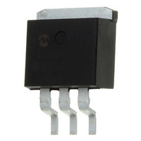
TC2117-3.0VEBTR Microchip Technology, TC2117-3.0VEBTR Datasheet - Page 4

TC2117-3.0VEBTR
Manufacturer Part Number
TC2117-3.0VEBTR
Description
IC CMSO LDO 3.0V 800MA DDPAK-3
Manufacturer
Microchip Technology
Specifications of TC2117-3.0VEBTR
Regulator Topology
Positive Fixed
Voltage - Output
3V
Voltage - Input
Up to 6V
Voltage - Dropout (typical)
1.2V @ 800mA
Number Of Regulators
1
Current - Output
800mA (Min)
Operating Temperature
-40°C ~ 125°C
Mounting Type
Surface Mount
Package / Case
TO-263-3, D²Pak (3 leads + Tab), TO-263AA
Number Of Outputs
1
Polarity
Positive
Input Voltage Max
6 V
Output Voltage
3 V
Output Type
Fixed
Dropout Voltage (max)
30 mV
Output Current
800 mA
Line Regulation
0.001 %
Load Regulation
0 % / mA
Voltage Regulation Accuracy
0.5 %
Maximum Operating Temperature
+ 125 C
Mounting Style
SMD/SMT
Minimum Operating Temperature
- 40 C
Lead Free Status / RoHS Status
Lead free / RoHS Compliant
Current - Limit (min)
-
Lead Free Status / Rohs Status
Lead free / RoHS Compliant
Other names
TC21173.0VEBTR
Available stocks
Company
Part Number
Manufacturer
Quantity
Price
Company:
Part Number:
TC2117-3.0VEBTR
Manufacturer:
MICROCHIP
Quantity:
6 000
Part Number:
TC2117-3.0VEBTR
Manufacturer:
MICROCHIP/微芯
Quantity:
20 000
TC2117
3.0
The TC2117 is a precision, positive output LDO. Unlike
bipolar regulators, the TC2117 supply current does not
increase proportionally with load current. In addition,
V
entire 0mA to 800mA operating load range.
FIGURE 3-1:
3.1
A 1µF (min) capacitor from V
The output capacitor should have an effective series
resistance of 0.2Ω to 10Ω. A 1µF capacitor should be
connected from V
inches of wire between the regulator and the AC filter
capacitor, or if a battery is used as the power source.
Aluminum electrolytic or tantalum capacitor types can
be used. (Since many aluminum electrolytic capacitors
freeze at approximately -30°C, solid tantalums are rec-
ommended for applications operating below -25°C.)
When operating from sources other than batteries, sup-
ply noise rejection and transient response can be
improved by increasing the value of the input and output
capacitors and employing passive filtering techniques.
3.2
3.2.1
Integrated thermal protection circuitry shuts the regula-
tor off when die temperature exceeds 160°C. The reg-
ulator remains off until the die temperature drops to
approximately 150°C.
DS21665B-page 4
OUT
Battery
remains stable and within regulation over the
DETAILED DESCRIPTION
Output Capacitor
Thermal Considerations
THERMAL SHUTDOWN
IN
C1
1µF
to GND if there is more than 10
TYPICAL APPLICATION
CIRCUIT
V
GND
IN
TC2117
OUT
V
to ground is required.
OUT
C2
1µF
V
OUT
3.2.2
The amount of power the regulator dissipates is prima-
rily a function of input and output voltage, and output
current. The following equation is used to calculate
worst case actual power dissipation:
EQUATION 3-1:
The
(Equation 3-2) is a function of the maximum ambient
temperature (T
perature (125°C) and the thermal resistance from
junction-to-air (θ
EQUATION 3-2:
Table 3-1 shows various values of θ
mounted on a 1/16 inch, 2-layer PCB with 1 oz. copper
foil.
TABLE 3-1:
*Tab of device attached to topside copper.
2500 sq mm
1000 sq mm
1000 sq mm
1000 sq mm
Where:
225 sq mm
100 sq mm
(Topside)*
I
Copper
V
LOAD
Area
V
OUT
IN
maximum
Where all terms are previously defined.
MAX
MAX
P
MIN
D
P
POWER DISSIPATION
D
= Worst case actual power dissipation
= Maximum voltage on V
= Maximum regulator output voltage
= Maximum output (load) current
≈ (V
2500 sq mm
2500 sq mm
2500 sq mm
2500 sq mm
1000 sq mm
A
(Backside)
MAX
JA
P
0 sq mm
Copper
D
Area
THERMAL RESISTANCE
GUIDELINES FOR TC2117 IN
3-PIN SOT-223 PACKAGE
).
IN
), the maximum allowable die tem-
MAX
MAX
allowable
=
©
– V
T
2002 Microchip Technology Inc.
J
MAX
OUT
2500 sq mm
2500 sq mm
2500 sq mm
2500 sq mm
1000 sq mm
1000 sq mm
Board Area
θ
– T
MIN
JA
power
)I
A
LOAD
MAX
JA
IN
for the TC2117
MAX
Resistance
Thermal
dissipation
45°C/W
45°C/W
53°C/W
59°C/W
52°C/W
55°C/W


