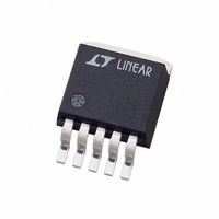
LT1185CQ#TR Linear Technology, LT1185CQ#TR Datasheet - Page 8

LT1185CQ#TR
Manufacturer Part Number
LT1185CQ#TR
Description
IC REG LDO ADJUSTABLE 3A DDPAK-5
Manufacturer
Linear Technology
Datasheet
1.LT1185CTPBF.pdf
(16 pages)
Specifications of LT1185CQ#TR
Regulator Topology
Negative Adjustable
Voltage - Output
-2.5 ~ -25 V
Voltage - Input
-4.2 ~ -35 V
Voltage - Dropout (typical)
0.67V @ 3A
Number Of Regulators
1
Current - Output
3A
Current - Limit (min)
Adjustable
Operating Temperature
0°C ~ 125°C
Mounting Type
Surface Mount
Package / Case
TO-263-5, D²Pak (5 leads + Tab), TO-263BA
Lead Free Status / RoHS Status
Contains lead / RoHS non-compliant
Available stocks
Company
Part Number
Manufacturer
Quantity
Price
8
APPLICATIO S I FOR ATIO
LT1185
factor is that local ambient temperature may be somewhat
higher because of the point source of heat. The conse-
quences of excess junction temperature include poor
reliability, especially for plastic packages, and the possi-
bility of thermal shutdown or degraded electrical charac-
teristics. The final design should be checked in situ with a
thermocouple attached to the regulator case under worst-
case conditions of high ambient, high input voltage and
full load.
What About Overloads?
IC regulators with thermal shutdown, like the LT1185,
allow heat sink designs which concentrate on worst-case
“normal” conditions and ignore “fault” conditions. An
output overload or short may force the regulator to exceed
its maximum junction temperature rating, but thermal
shutdown is designed to prevent regulator failure under
these conditions. A word of caution however; thermal
shutdown temperatures are typically 175°C in the control
portion of the die and 180°C to 225°C in the power
transistor section. Extended operation at these tempera-
tures can cause permanent degradation of plastic encap-
sulation. Designs which may be subjected to extended
periods of overload should either use the hermetic TO-3
package or increase heat sink size. Foldback current
limiting can be implemented to minimize power levels
under fault conditions.
External Current Limit
The LT1185 requires a resistor to set current limit. The
value of this resistor is 15k divided by the desired current
limit (in amps). The resistor for 2A current limit would be
15k/2A = 7.5k. Tolerance over temperature is ±10%, so
current limit is normally set 15% above maximum load
current. Foldback limiting can be employed if short-circuit
current must be lower than full load current (see Typical
Applications).
The LT1185 has internal current limiting which will over-
ride external current limit if power in the pass transistor
is excessive. The internal limit is ≈ 3.6A with a foldback
characteristic which is dependent on input-output volt-
age, not output voltage per se (see Typical Performace
Characteristics).
U
U
W
U
Ground Pin Current
Ground pin current for the LT1185 is approximately 2mA
plus I
2mA + 3/40 = 77mA. Worst case guarantees on the ratio of
I
Specifications.
Ground pin current can be important for two reasons. It
adds to power dissipation in the regulator and it can affect
load/line regulation if a long line is run from the ground pin
to load ground. The additional power dissipation is found
by multiplying ground pin current by input voltage. In a
typical example, with V
LT1185 will dissipate (8V – 5V)(2A) = 6W in the pass
transistor and (2A/40)(8V) = 0.4W in the internal drive
circuitry. This is only a 1.5% efficiency loss, and a 6.7%
increase in regulator power dissipation, but these values
will increase at higher output voltages.
Ground pin current can affect regulation as shown in
Figure 2. Parasitic resistance in the ground pin lead will
create a voltage drop which increases output voltage as
load current is increased. Similarly, output voltage can
decrease as input voltage increases because the “I
component of ground pin current drops significantly at
higher input-output differentials. These effects are small
enough to be ignored for local regulation applications, but
OUT
V
+
–
*R1 SHOULD BE CONNECTED DIRECTLY TO GROUND LEAD, NOT TO THE LOAD,
IN
SO THAT r
ERRORS CREATED BY r
INCREASES WITH INCREASING GROUND PIN CURRENT. R2 SHOULD BE CONNECTED
DIRECTLY TO LOAD FOR REMOTE SENSING
to ground pin current are contained in the Electrical
OUT
Figure 2. Proper Connection of Positive Sense Lead
V
a
/40. At I
IN
≈ 0Ω. THIS LIMITS THE OUTPUT VOLTAGE ERROR TO (I
REF
R
LIM
LT1185
OUT
a
ARE MULTIPLIED BY (1 + R2/R1). NOTE THAT V
= 3A, ground pin current is typically
GND
IN
V
= 8V, V
OUT
FB
LEAD RESISTANCES
r
a
PARASITIC
OUT
= 5V and I
R1*
2.37k
R2
– r
I
GND
b
+
OUT
LOAD
GND
)(r
= 2A, the
OUT
OUT
b
).
LT1185 • F02
/40”
1185ff
V
OUT
+
–


