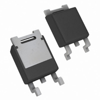
LMS8117ADT-ADJ/NOPB National Semiconductor, LMS8117ADT-ADJ/NOPB Datasheet - Page 9

LMS8117ADT-ADJ/NOPB
Manufacturer Part Number
LMS8117ADT-ADJ/NOPB
Description
IC REGULATOR 1A LDO TO-252
Manufacturer
National Semiconductor
Datasheet
1.LMS8117AMPX-1.8NOPB.pdf
(16 pages)
Specifications of LMS8117ADT-ADJ/NOPB
Regulator Topology
Positive Adjustable
Voltage - Output
1.25 ~ 13.8 V
Voltage - Input
Up to 15V
Voltage - Dropout (typical)
1.2V @ 1A
Number Of Regulators
1
Current - Output
1A
Current - Limit (min)
1A
Operating Temperature
0°C ~ 125°C
Mounting Type
Surface Mount
Package / Case
TO-252-2, DPak (2 Leads + Tab), TO-252AA, SC-63
Lead Free Status / RoHS Status
Lead free / RoHS Compliant
Other names
*LMS8117ADT-ADJ
*LMS8117ADT-ADJ/NOPB
LMS8117ADT-ADJ
*LMS8117ADT-ADJ/NOPB
LMS8117ADT-ADJ
Available stocks
Company
Part Number
Manufacturer
Quantity
Price
Part Number:
LMS8117ADT-ADJ/NOPB
Manufacturer:
TI/德州仪器
Quantity:
20 000
Application Note
The LMS8117A regulators have internal thermal shutdown to
protect the device from over-heating. Under all possible
operating conditions, the junction temperature of the
LMS8117A must be within the range of 0˚C to 125˚C. A
heatsink may be required depending on the maximum power
dissipation and maximum ambient temperature of the appli-
cation. To determine if a heatsink is needed, the power
dissipated by the regulator, P
Figure 6 shows the voltages and currents which are present
in the circuit.
The next parameter which must be calculated is the maxi-
mum allowable temperature rise, T
I
P
IN
D
= I
FIGURE 5. Cross-sectional view of Integrated Circuit Mounted on a printed circuit board. Note that the case
= (V
L
FIGURE 6. Power Dissipation Diagram
+ I
IN
-V
G
temperature is measured at the point where the leads contact with the mounting pad surface
OUT
)I
L
+ V
IN
I
G
D
(Continued)
, must be calculated:
R
(max):
10119616
9
where T
ture (125˚C), and T
perature which will be encountered in the application.
Using the calculated values for T
mum allowable value for the junction-to-ambient thermal
resistance (θ
If the maximum allowable value for θ
≥136˚C/W for SOT-223 package or ≥92˚C/W for TO-252
package, no heatsink is needed since the package alone will
dissipate enough heat to satisfy these requirements. If the
calculated value for θ
required.
As a design aid, Table 1 shows the value of the θ
SOT-223 and TO-252 for different heatsink area. The copper
patterns that we used to measure these θ
the end of the Application Notes Section. Figure 7 and Figure
8 reflects the same test results as what are in the Table 1.
Figure 9 and Figure 10 shows the maximum allowable power
dissipation vs. ambient temperature for the SOT-223 and
TO-252 device. Figure 11 and Figure 12 shows the maxi-
mum allowable power dissipation vs. copper area (in
the SOT-223 and TO-252 devices. Please see AN–1028 for
power enhancement techniques to be used with SOT-223
and TO-252 packages.
T
θ
JA
R
(max)=T
= T
J
(max) is the maximum allowable junction tempera-
R
(max)/P
JA
J
(max)-T
) can be calculated:
D
A
JA
(max) is the maximum ambient tem-
A
(max)
falls below these limits, a heatsink is
R
10119637
(max) and P
JA
JA
is found to be
s are shown at
D
www.national.com
, the maxi-
2
JA
) for
of


