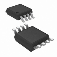
LP2966IMM-1833/NOPB National Semiconductor, LP2966IMM-1833/NOPB Datasheet - Page 4

LP2966IMM-1833/NOPB
Manufacturer Part Number
LP2966IMM-1833/NOPB
Description
IC REG DUAL ULTRA LDO 8-MSOP
Manufacturer
National Semiconductor
Datasheet
1.LP2966IMM-5050NOPB.pdf
(15 pages)
Specifications of LP2966IMM-1833/NOPB
Regulator Topology
Positive Fixed
Voltage - Output
1.8V, 3.3V
Voltage - Input
2.7 ~ 7 V
Voltage - Dropout (typical)
-, 0.135V @ 150mA
Number Of Regulators
2
Current - Output
150mA
Operating Temperature
-40°C ~ 125°C
Mounting Type
Surface Mount
Package / Case
8-MSOP, Micro8™, 8-uMAX, 8-uSOP,
Lead Free Status / RoHS Status
Lead free / RoHS Compliant
Current - Limit (min)
-
Other names
LP2966IMM-1833
LP2966IMM-1833TR
LP2966IMM-1833TR
Available stocks
Company
Part Number
Manufacturer
Quantity
Price
Company:
Part Number:
LP2966IMM-1833/NOPB
Manufacturer:
ST
Quantity:
43 000
www.national.com
V
(Note 13)
∆V
(Note 8)
(Note 13)
∆V
∆V
V
I
I
I
I
Short Circuit Foldback Protection
I
Over Temperature Protection
Tsh(t)
GND(1,0)
GND(1,1)
GND(0,0)
O(PK)
FB
o
IN
Absolute Maximum Ratings
If Military/Aerospace specified devices are required,
please contact the National Semiconductor Sales Office/
Distributors for availability and specifications.
Electrical Characteristics
Limits in standard typeface are for T
range. Unless otherwise specified, V
Storage Temperature Range
Lead Temp. (Soldering, 5 sec.)
Power Dissipation (Note 2)
ESD Rating (Note 3)
Input Supply Voltage (Survival)
Shutdown Input Voltage (Survival)
Maximum Voltage for ERROR Pins
I
O
O
O2
OUT
-V
/∆V
/∆I
/∆I
Symbol
OUT
OUT
(Survival)
IN
OUT1
(Note 18)
Output Voltage
Tolerance
Output Voltage Line
Regulation
Output Voltage Load
Regulation (Note 9)
Output Voltage Cross
Regulation (Note 10)
Dropout Voltage
(Note 12)
Ground Pin Current
(One LDO On)
Ground Pin Current
(Both LDOs On)
Ground Pin Current
in Shutdown Mode
Peak Output Current
Short Circuit
Foldback Knee
Shutdown Threshold
Parameter
j
IN
= 25˚C, and limits in boldface type apply over the full operating junction temperature
Short Circuit Protected
−0.3V to (Vin + 0.3V)
= V
O(NOM)
Internally Limited
V
1mA
1mA
(Note 9)
1mA
(Note 10)
I
I
I
I
V
I
V
I
I
V
(Note 2)
V
(Note 2), (Note 14)
L
L
L
L
L
L
L
OUT
SD2
SD2
SD1
OUT
−65 to +150˚C
= 1mA
= 100mA
= 150mA
= 1mA
= 100mA
= 1mA
= 100mA
−0.3V to 7.5V
(Note 1)
= V
≥ V
<
<
<
≤ 0.1V, V
≤ 0.1V, V
+ 1V
+ 1V, (Note 16), C
I
I
I
Conditions
L
L
L1
SD2
OUT(NOM)
<
<
260˚C
<
<
100mA
10V
2kV
100mA
≤ 0.1V
100mA
V
SD1
SD1
IN
- 5%
<
= V
= V
4
7.0V
IN
IN
Operating Ratings
Output Voltage (Survival)(Note 6),
(Note 7)
Input Supply Voltage
Shutdown Input Voltage
Operating Junction
Temperature Range
Maximum Voltage for ERROR
pins
OUT
= 1µF, I
Typ (Note
0.0004
0.006
135
300
340
340
420
500
600
165
0.0
0.0
0.1
0.1
0.9
90
4)
OUT
= 1mA, C
LP2966IMM (Note 5)
−1.5
Min
-3.5
350
150
−1
-3
IN
= 1µF, V
(Note 1)
−0.3V to (Vin + 0.3V)
−0.3V to (Vin + 0.3V)
SD1
Max
130
180
195
270
450
500
540
600
1.5
3.5
2.0
3.0
0.3
10
1
3
−40˚C to +125˚C
= V
2.7V to 7.0V
SD2
= V
%V
%V
mV/mA
mV/mA
mV/V
Unit
mV
mA
mA
µA
µA
µA
˚C
10V
NOM
NOM
IN
.


