LP38852MRX-ADJ/NOPB National Semiconductor, LP38852MRX-ADJ/NOPB Datasheet - Page 4

LP38852MRX-ADJ/NOPB
Manufacturer Part Number
LP38852MRX-ADJ/NOPB
Description
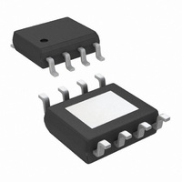
IC REG LDO 1.5A ADJ FAST 8-PSOP
Manufacturer
National Semiconductor
Series
PowerWise®r
Datasheet
1.LP38852EVAL.pdf
(18 pages)
Specifications of LP38852MRX-ADJ/NOPB
Regulator Topology
Positive Adjustable
Voltage - Output
0.8 ~ 1.8 V
Voltage - Input
0.93 ~ 5.5 V
Voltage - Dropout (typical)
0.13V @ 1.5A
Number Of Regulators
1
Current - Output
1.5A (Max)
Operating Temperature
-40°C ~ 125°C
Mounting Type
Surface Mount
Package / Case
8-PSOP
For Use With
LP38852EVAL - BOARD EVALUATION LP38852
Lead Free Status / RoHS Status
Lead free / RoHS Compliant
Current - Limit (min)
-
Other names
LP38852MRX-ADJ
Available stocks
Company
Part Number
Manufacturer
Quantity
Price
Company:
Part Number:
LP38852MRX-ADJ/NOPB
Manufacturer:
NS
Quantity:
700
www.national.com
Soft-Start
Enable
AC Parameters
Thermal Parameters
Note 1: Note 1: Absolute Maximum Ratings indicate limits beyond which damage to the device may occur. Operating Ratings indicate conditions for which the
device is intended to be functional, but does not guarantee specific performance limits. For guaranteed specifications and conditions, see the Electrical
Characteristics.
Note 2: The human body model is a 100 pF capacitor discharged through a 1.5k resistor into each pin. Test method is per JESD22-A114.
Note 3: Device power dissipation must be de-rated based on device power dissipation (P
resistance (θ
the Application Information section for details.
Note 4: Output voltage line regulation is defined as the change in output voltage from nominal value resulting from a change in input voltage.
Note 5: Output voltage load regulation is defined as the change in output voltage from nominal value as the load current increases from no load to full load.
Note 6: Dropout voltage is defined the as input to output voltage differential (V
drop 2% from the nominal value.
Note 7: V
Symbol
V
T
V
(V
PSRR
PSRR
SD(HYS)
EN(HYS)
(V
EN(ON)
t
θ
θ
T
t
r
t
I
OFF
BIAS
e
ON
SS
EN
SS
J-A
J-C
SD
IN
n
)
)
IN
cannot exceed either V
JA
). Additional heat-sinking may be required to ensure that the device junction temperature (T
Soft-Start internal resistance
Soft-Start time
t
ENABLE pin Current
Enable Voltage Threshold
Enable Voltage Hysteresis
Turn-OFF Delay Time
Turn-ON Delay Time
Ripple Rejection for V
Voltage
Ripple Rejection for V
Output Noise Density
Output Noise Voltage
Thermal Shutdown Junction
Temperature
Thermal Shutdown Hysteresis
Thermal Resistance, Junction to
Ambient
Thermal Resistance, Junction to
Case
SS
= C
(Note
SS
(Note
× r
Parameter
3)
SS
3)
BIAS
× 5
or 4.5V, whichever value is lower.
IN
BIAS
Input
Voltage
C
V
V
V
V
OFF
R
R
V
f = 120 Hz
V
f = 1 kHz
V
f = 120 Hz
V
f = 1 kHz
f = 120 Hz
BW = 10 Hz − 100 kHz
BW = 300 Hz − 300 kHz
TO220-7
TO263-7
PSOP-8
TO220-7
TO263-7
PSOP-8
EN
EN
EN
EN
IN
IN
BIAS
BIAS
SS
LOAD
LOAD
= V
= V
= 10 nF
= V
= 0.0V, V
rising until Output = ON
falling from V
= V
= V
x C
x C
OUT(NOM)
OUT(NOM)
BIAS
OUT(NOM)
OUT(NOM)
OUT
OUT
Conditions
BIAS
<< t
<< t
IN
4
- V
+ 1V,
+ 1V,
EN(ON)
OFF
ON
= 5.5V
+ 3V,
+ 3V,
OUT
) where the input voltage is low enough to cause the output voltage to
D
), ambient temperature (T
until Output =
J
) does not exceed the maximum operating rating. See
11.0
1.00
0.90
MIN
-19
-13
50
30
-
-
-
-
-
-
-
-
-
-
-
-
-
-
-
-
-
-
-
A
), and package junction to ambient thermal
TYP
13.5
0.01
1.25
675
100
150
160
168
-30
20
15
80
65
58
58
90
10
60
60
11
1
3
3
MAX
16.0
1.50
1.55
150
200
-40
-51
-
-
-
-
-
-
-
-
-
-
-
-
-
-
-
-
-
-
-
µV/
µV
Units
°C/W
mV
kΩ
μA
dB
°C
μs
µs
V
√
RMS
Hz


