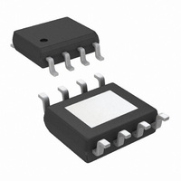
LP38852MR-ADJ/NOPB National Semiconductor, LP38852MR-ADJ/NOPB Datasheet - Page 11

LP38852MR-ADJ/NOPB
Manufacturer Part Number
LP38852MR-ADJ/NOPB
Description
IC REG LDO 1.5A LOW I/O 8-PSOP
Manufacturer
National Semiconductor
Series
PowerWise®r
Datasheet
1.LP38852EVAL.pdf
(18 pages)
Specifications of LP38852MR-ADJ/NOPB
Regulator Topology
Positive Adjustable
Voltage - Output
0.8 ~ 1.8 V
Voltage - Input
0.93 ~ 5.5 V
Voltage - Dropout (typical)
0.13V @ 1.5A
Number Of Regulators
1
Current - Output
1.5A (Max)
Operating Temperature
-40°C ~ 125°C
Mounting Type
Surface Mount
Package / Case
8-PSOP
For Use With
LP38852EVAL - BOARD EVALUATION LP38852
Lead Free Status / RoHS Status
Lead free / RoHS Compliant
Current - Limit (min)
-
Other names
LP38852MR-ADJ
Available stocks
Company
Part Number
Manufacturer
Quantity
Price
Application Information
EXTERNAL CAPACITORS
To assure regulator stability, input and output capacitors are
required as shown in the Typical Application Circuit.
Output Capacitor
A minimum output capacitance of 10 µF, ceramic, is required
for stability. The amount of output capacitance can be in-
creased without limit. The output capacitor must be located
less than 1 cm from the output pin of the IC and returned to
the device ground pin with a clean analog ground.
Only high quality ceramic types such as X5R or X7R should
be used, as the Z5U and Y5F types do not provide sufficient
capacitance over temperature.
Tantalum capacitors will also provide stable operation across
the entire operating temperature range. However, the effects
of ESR may provide variations in the output voltage during
fast load transients. Using the minimum recommended 10 µF
ceramic capacitor at the output will allow unlimited capaci-
tance, Tantalum and/or Aluminum, to be added in parallel.
Input Capacitor
The input capacitor must be at least 10 µF, but can be in-
creased without limit. It's purpose is to provide a low source
impedance for the regulator input. A ceramic capacitor, X5R
or X7R, is recommended.
Tantalum capacitors may also be used at the input pin. There
is no specific ESR limitation on the input capacitor (the lower,
the better).
Aluminum electrolytic capacitors can be used, but are not
recommended as their ESR increases very quickly at cold
temperatures. They are not recommended for any application
where the ambient temperature falls below 0°C.
Bias Capacitor
The capacitor on the bias pin must be at least 1 µF, and can
be any good quality capacitor (ceramic is recommended).
Feed Forward Capacitor, C
(Refer to the Typical Application Circuit)
When using a ceramic capacitor for C
value will be too small to provide any meaningful positive
phase compensation, F
shifts in the gain loop.
A capacitor placed across the gain resistor R1 will provide
additional phase margin to improve load transient response
of the device. This capacitor, C
a zero in the loop response given by the formula:
For optimum load transient response select C
frequency, F
F
Z
Z
F
(C
, falls between 10 kHz and 15 kHz.
= (1 / (2 x
Z
FF
= (1 / (2 x
= (1 / (2 x
Z
, to offset the internal negative phase
π
π
x C
π
x C
FF
OUT
FF
x R1 x F
FF
, in parallel with R1, will form
x ESR) )
x R1) )
OUT
Z
)
, the typical ESR
FF
so the zero
(1)
(2)
(3)
11
The phase lead provided by C
approaches unity, or V
C
It's important to note that at higher output voltages, where R1
is much larger than R2, the pole and zero are far apart in fre-
quency. At lower output voltages the frequency of the pole
and the zero mover closer together. The phase lead provided
from C
and has no effect when V
on this compensation technique alone is adequate only for
higher output voltages. For the LP38852, the practical mini-
mum V
C
SETTING THE OUTPUT VOLTAGE
(Refer to the Typical Application Circuit)
The output voltage is set using the external resistive divider
R1 and R2. The output voltage is given by the formula:
The resistors used for R1 and R2 should be high quality, tight
tolerance, and with matching temperature coefficients. It is
important to remember that, although the value of V
guaranteed, the use of low quality resistors for R1 and R2 can
easily produce a V
It is recommended that the values selected for R1 and R2 are
such that the parallel value is less than 10 kΩ. This is to pre-
vent internal parasitic capacitances on the ADJ pin from
interfering with the F
Table 1
values for R1 and R2, and a standard ±10% capacitor values
for C
and C
FF
OUT
also forms a pole with a frequency of:
FF
.
FF
FF
, for a range of V
OUT
lists some suggested, best fit, standard ±1% resistor
are available that will give similar results.
F
diminishes quickly as the output voltage is reduced,
P
( (R1 x R2) / (R1 + R2) )
FIGURE 1. F
= (1 / (2 x
is 0.8V when a ceramic capacitor is used for
OUT
Z
pole set by R1 and C
π
OUT
value that is unacceptable.
OUT
ZERO
x C
OUT
approaches V
FF
values. Other values of R1, R2,
= V
and F
FF
x (R1 || R2) ) )
ADJ
diminishes as the DC gain
≤
POLE
. For this reason, relying
10 kΩ
ADJ
vs Gain
FF
. This is because
.
20213921
www.national.com
ADJ
(4)
(5)
(6)
is


