NCP508SQ15T1G ON Semiconductor, NCP508SQ15T1G Datasheet - Page 12
NCP508SQ15T1G
Manufacturer Part Number
NCP508SQ15T1G
Description
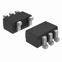
IC REG LDO 50MA 1.5V SC-88A
Manufacturer
ON Semiconductor
Datasheet
1.NCP508SQ15T1G.pdf
(15 pages)
Specifications of NCP508SQ15T1G
Regulator Topology
Positive Fixed
Voltage - Output
1.5V
Voltage - Input
Up to 7V
Voltage - Dropout (typical)
0.18V @ 50mA
Number Of Regulators
1
Current - Output
50mA (Min)
Operating Temperature
-40°C ~ 85°C
Mounting Type
Surface Mount
Package / Case
SC-70-5, SC-88A, SOT-353, 16-QFN, SC-70-6, SC-88, SOT-323-6, SOT-363, SOT-23-8
Number Of Outputs
1
Polarity
Positive
Input Voltage Max
13 V
Output Voltage
1.5 V
Output Voltage Tolerance
3 %
Output Type
Fixed
Dropout Voltage (max)
300 mV
Output Current
50 mA
Line Regulation
2 mV
Load Regulation
6 mV
Maximum Operating Temperature
+ 85 C
Mounting Style
SMD/SMT
Minimum Operating Temperature
- 40 C
Lead Free Status / RoHS Status
Lead free / RoHS Compliant
Current - Limit (min)
-
Available stocks
Company
Part Number
Manufacturer
Quantity
Price

Part Number:
NCP508SQ15T1G
Manufacturer:
ON/安森美
Quantity:
20 000


Load Regulation
current at a constant temperature.
Dropout Voltage
no longer maintains regulation against further reductions in
input voltage. Measured when the output drops 100 mV
below its nominal. The junction temperature, load current,
and minimum input supply requirements affect the dropout
level.
Maximum Power Dissipation
will operate within its specifications.
Quiescent Current
the ground when the LDO operates without a load on its
output: internal IC operation, bias, etc. When the LDO
becomes loaded, this term is called the Ground current. It is
actually the difference between the input current (measured
through the LDO input pin) and the output current.
in Figure 1.
Input Decoupling (C1)
is recommended to improve the transient response of the
regulator and/or if the regulator is located more than a few
inches from the power source. It will also reduce the circuit’s
sensitivity to the input line impedance at high frequencies.
The capacitor should be mounted with the shortest possible
track length directly across the regular’s input terminals.
Higher values and lower ESR will improve the overall line
transient response.
Output Decoupling (C2)
minimum output current. Capacitors exhibiting ESRs
ranging from a few mW up to 3 W can safely be used. The
minimum decoupling value is 1.0 mF and can be augmented
to fulfill stringent load transient requirements. The regulator
accepts ceramic chip capacitors as well as tantalum devices.
Larger values improve noise rejection and load regulation
transient response.
Enable Operation
of threshold are covered in the electrical specification
section of this datasheet. If the enable is not used then the pin
should be connected to V
The change in output voltage for a change in output
The input/output differential at which the regulator output
The maximum total dissipation for which the regulator
The quiescent current is the current which flows through
Typical application circuit for the NCP508 series is shown
An input capacitor of at least 1.0 mF,(ceramic or tantalum)
The NCP508 is a stable regulator and does not require a
The enable pin will turn on or off the regulator. The limits
in
.
APPLICATIONS INFORMATION
http://onsemi.com
DEFINITIONS
12
Line Regulation
The measurement is made under conditions of low
dissipation or by using pulse technique such that the average
chip temperature is not significantly affected.
Line Transient Response
is excited with a given slope.
Thermal Protection
the integrated circuit in the event that the maximum junction
temperature is exceeded. When activated at typically 125°C,
the regulator turns off. This feature is provided to prevent
failures from accidental overheating.
Maximum Package Power Dissipation
dissipation level at which the junction temperature reaches
its maximum operating value, i.e. 150°C. Depending on the
ambient power dissipation and thus the maximum available
output current.
Hints
When the impedance of these lines is high, there is a chance
to pick up noise or cause the regulator to malfunction.
as close as possible to the circuit, and make leads as short as
possible.
Thermal Considerations
the integrated circuit in the event that the maximum junction
temperature is exceeded.
is dependent upon board design and layout. Mounting pad
configuration on the PCB, the board material and also the
ambient temperature effect the rate of temperature rise for
the part. This is stating that when the NCP508 has good
thermal conductivity through the PCB, the junction
temperature will be relatively low with high power
dissipation applications.
by:
where:
− T
− T
− R
The change in output voltage for a change in input voltage.
Typical over and undershoot response when input voltage
Internal thermal shutdown circuitry is provided to protect
The maximum power package dissipation is the power
Please be sure the V
Set external components, especially the output capacitor,
Internal thermal limiting circuitry is provided to protect
The maximum power dissipation supported by the device
The maximum dissipation the package can handle is given
of the die, which is 150°C
A
J{max)
qja
is the ambient operating temperature
is dependent on the surrounding PCB layout
is the maximum allowable junction temperature
P
in
D
+
and GND lines are sufficiently wide.
T
J
(
max
R
qJA
)
* T
A
(eq. 1)
Related parts for NCP508SQ15T1G
Image
Part Number
Description
Manufacturer
Datasheet
Request
R

Part Number:
Description:
ON Semiconductor [VOLTAGE REGULATOR]
Manufacturer:
ON Semiconductor
Datasheet:
Part Number:
Description:
357-036-542-201 CARDEDGE 36POS DL .156 BLK LOPRO
Manufacturer:
ON Semiconductor
Datasheet:
Part Number:
Description:
357-036-542-201 CARDEDGE 36POS DL .156 BLK LOPRO
Manufacturer:
ON Semiconductor
Datasheet:
Part Number:
Description:
357-036-542-201 CARDEDGE 36POS DL .156 BLK LOPRO
Manufacturer:
ON Semiconductor
Datasheet:
Part Number:
Description:
357-036-542-201 CARDEDGE 36POS DL .156 BLK LOPRO
Manufacturer:
ON Semiconductor
Datasheet:
Part Number:
Description:
357-036-542-201 CARDEDGE 36POS DL .156 BLK LOPRO
Manufacturer:
ON Semiconductor
Datasheet:
Part Number:
Description:
357-036-542-201 CARDEDGE 36POS DL .156 BLK LOPRO
Manufacturer:
ON Semiconductor
Datasheet:
Part Number:
Description:
357-036-542-201 CARDEDGE 36POS DL .156 BLK LOPRO
Manufacturer:
ON Semiconductor
Datasheet:
Part Number:
Description:
357-036-542-201 CARDEDGE 36POS DL .156 BLK LOPRO
Manufacturer:
ON Semiconductor
Datasheet:
Part Number:
Description:
357-036-542-201 CARDEDGE 36POS DL .156 BLK LOPRO
Manufacturer:
ON Semiconductor
Datasheet:
Part Number:
Description:
357-036-542-201 CARDEDGE 36POS DL .156 BLK LOPRO
Manufacturer:
ON Semiconductor
Datasheet:
Part Number:
Description:
Manufacturer:
ON Semiconductor
Datasheet:
Part Number:
Description:
Manufacturer:
ON Semiconductor
Datasheet:
Part Number:
Description:
Manufacturer:
ON Semiconductor
Datasheet: