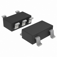
NCP561SN50T1G ON Semiconductor, NCP561SN50T1G Datasheet - Page 3

NCP561SN50T1G
Manufacturer Part Number
NCP561SN50T1G
Description
IC REG LDO 150MA 5.0V SOT23-5
Manufacturer
ON Semiconductor
Datasheet
1.NCP561SN15T1G.pdf
(10 pages)
Specifications of NCP561SN50T1G
Regulator Topology
Positive Fixed
Voltage - Output
5V
Voltage - Input
Up to 6V
Voltage - Dropout (typical)
0.12V @ 150mA
Number Of Regulators
1
Current - Output
150mA (Min)
Operating Temperature
-40°C ~ 85°C
Mounting Type
Surface Mount
Package / Case
TSOT-23-5, TSOT-5, TSOP-5
Number Of Outputs
1
Polarity
Positive
Input Voltage Max
6 V
Output Voltage
5 V
Output Type
Fixed
Dropout Voltage (max)
0.19 V at 150 mA
Output Current
150 mA
Line Regulation
20 mV
Load Regulation
60 mV
Voltage Regulation Accuracy
2 %
Maximum Operating Temperature
+ 85 C
Mounting Style
SMD/SMT
Minimum Operating Temperature
- 40 C
Lead Free Status / RoHS Status
Lead free / RoHS Compliant
Current - Limit (min)
-
Lead Free Status / Rohs Status
Lead free / RoHS Compliant
Other names
NCP561SN50T1GOS
Available stocks
Company
Part Number
Manufacturer
Quantity
Price
Part Number:
NCP561SN50T1G
Manufacturer:
ON/安森美
Quantity:
20 000
3. Maximum package power dissipation limits must be observed.
4. Low duty cycle pulse techniques are used during testing to maintain the junction temperature as close to ambient as possible.
ELECTRICAL CHARACTERISTICS
unless otherwise noted.)
Output Voltage (T
Line Regulation
Load Regulation (I
Output Current (V
Dropout Voltage (T
Quiescent Current
Output Short Circuit Current
Output Voltage Noise
Enable Input Threshold Voltage
Output Voltage Temperature Coefficient
1.5 V
1.8 V
2.5 V
2.7 V
2.8 V
3.0 V
3.3 V
5.0 V
1.5 V-4.4 V (V
4.5 V-5.0 V (V
1.5 V to 3.9 V (V
4.0 V to 5.0 V (V
Measured at V
1.5 V - 1.7 V
1.8 V - 2.4 V
2.5 V - 2.7 V
2.8 V - 3.2 V
3.3 V - 4.9 V
5.0 V
(Enable Input = 0 V)
(Enable Input = V
1.5 V to 3.9 V (V
4.0 V to 5.0 V (V
(f = 20 Hz to 100 kHz, V
(Voltage Increasing, Output Turns On, Logic High)
(Voltage Decreasing, Output Turns Off, Logic Low)
PD +
T J(max) *T A
IN
IN
OUT
R qJA
A
IN
IN
IN
IN
OUT
= V
= 5.5 V to 6.0 V)
OUT
IN
A
= 25°C, I
= V
= 6.0 V)
= V
= 6.0 V)
- 3.0%)
, I
= -40°C to 85°C, I
o(nom)
OUT
= (V
= 10 mA to 150 mA)
o(nom)
o(nom)
OUT
OUT
= 1.0 mA to I
Characteristic
OUT
+ 1.0 V to 6.0 V)
= 3.0, V I
+ 2.0 V)
+ 2.0 V)
at I
= 1.0 mA)
out
= 150 mA) -3.0%)
OUT
OUT
o(nom)
(V
= 150 mA,
= 1.0 V)
IN
)
= V
OUT(nom)
http://onsemi.com
+ 1.0 V, V
NCP561
3
enable
V
I
Symbol
OUT(max)
Reg
= V
Reg
IN
I
V
V
o(nom)
-V
th(en)
T
OUT
V
I
Q
IN
C
load
n
line
OUT
, C
IN
= 1.0 mF, C
1.455
1.746
2.425
2.646
2.744
2.940
3.234
4.90
Min
150
150
160
160
1.3
-
-
-
-
-
-
-
-
-
-
-
-
-
-
OUT
= 1.0 mF, T
"100
Typ
330
240
150
140
130
120
400
400
1.5
1.8
2.5
2.7
2.8
3.0
3.3
5.0
0.1
4.0
10
10
30
60
-
-
-
-
J
= 25°C,
1.545
1.854
2.575
2.754
2.856
3.060
3.366
Max
5.10
500
360
250
230
200
190
800
800
1.0
8.0
0.2
20
20
60
-
-
-
-
-
ppm/°C
mVrms
Unit
mV
mV
mA
mV
mA
mA
V
V


