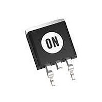
NCV317BD2TG ON Semiconductor, NCV317BD2TG Datasheet - Page 6

NCV317BD2TG
Manufacturer Part Number
NCV317BD2TG
Description
IC REG POS 1.5A ADJ OUT D2PAK
Manufacturer
ON Semiconductor
Datasheet
1.NCP317BTG.pdf
(12 pages)
Specifications of NCV317BD2TG
Regulator Topology
Positive Adjustable
Voltage - Output
1.2 ~ 37 V
Voltage - Input
Up to 40V
Number Of Regulators
1
Current - Output
500mA
Current - Limit (min)
1.5A
Operating Temperature
-40°C ~ 125°C
Mounting Type
Surface Mount
Package / Case
TO-263-2, D⊃2Pak (2 leads + Tab), TO-263AB
Polarity
Positive
Number Of Outputs
1
Output Type
Adjustable
Output Voltage
1.2 V to 37 V
Output Current
1.5 A
Line Regulation
0.04 % / V
Load Regulation
0.5 % / V
Input Voltage Max
40 V
Maximum Operating Temperature
+ 150 C
Minimum Operating Temperature
- 55 C
Mounting Style
SMD/SMT
Reference Voltage
1.3 V
Rohs Compliant
YES
Lead Free Status / RoHS Status
Lead free / RoHS Compliant
Voltage - Dropout (typical)
-
Lead Free Status / Rohs Status
Lead free / RoHS Compliant
Other names
NCV317BD2TGOS
Available stocks
Company
Part Number
Manufacturer
Quantity
Price
Company:
Part Number:
NCV317BD2TG
Manufacturer:
ON Semiconductor
Quantity:
1 954
Part Number:
NCV317BD2TG
Manufacturer:
ON/安森美
Quantity:
20 000
100
100
-0.5
-1.0
-1.5
80
60
40
20
80
60
40
20
1.5
1.0
0.5
1.0
0.5
0
0
10
0
0
0
Figure 15. Ripple Rejection versus Frequency
Figure 13. Ripple Rejection versus Output
5.0
100
0
Figure 17. Line Transient Response
V
I
T
V
I
f = 120 Hz
T
L
L
out
J
in
J
= 50 mA
= 500 mA
= 25°C
= 25°C
- V
= 10 V
1.0 k 10 k
10
out
V
= 5 V
10
out
f, FREQUENCY (Hz)
, OUTPUT VOLTAGE (V)
15
Voltage
t, TIME (ms)
100 k
20
20
C
C
1.0 M 10 M
L
Adj
25
= 1.0 mF;
C
I
V
V
T
= 10 mF
V
Without C
L
C
Without C
out
J
Adj
in
in
= 500 mA
Adj
= 25°C
= 15 V
30
= 10 V
= 10 mF
30
= 10 mF
C
Without C
L
Adj
= 0;
Adj
35
http://onsemi.com
Adj
40
6
10
10
10
10
10
-1.0
-2.0
-3.0
120
100
-1
-2
-3
3.0
2.0
1.0
1.5
1.0
0.5
80
60
40
20
1
0
0
10
0
0
0.01
V
V
f = 120 Hz
T
in
out
J
= 25°C
C
C
= 15 V
= 10 V
0
L
Adj
V
V
I
T
Without C
L
Figure 18. Load Transient Response
out
J
= 1.0 mF;
in
Figure 14. Ripple Rejection versus
= 500 mA
= 25°C
= 10 mF
= 15 V
100
= 10 V
Figure 16. Output Impedance
Adj
C
Without C
L
10
I
= 0;
O
0.1
, OUTPUT CURRENT (A)
f, FREQUENCY (Hz)
Output Current
1.0 k
Adj
t, TIME (ms)
20
C
Adj
10 k
= 10 mF
I
L
V
V
I
T
1.0
NL
out
J
in
30
C
Without C
= 25°C
= 15 V
= 50 mA
Adj
= 10 V
100 k
= 10 mF
Adj
40
1.0 M
10


