NCP605MN15T2G ON Semiconductor, NCP605MN15T2G Datasheet
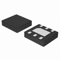
IC REG LDO 500MA 1.5V 6-DFN

NCP605MN15T2G

Manufacturer Part Number
NCP605MN15T2G
Description
IC REG LDO 500MA 1.5V 6-DFN
Manufacturer
ON Semiconductor
Datasheet

Specifications of NCP605MN15T2G

Regulator Topology
Positive Fixed
Voltage - Output
1.5V
Voltage - Input
Up to 6V
Voltage - Dropout (typical)
0.29V @ 500mA
Number Of Regulators
1
Current - Output
500mA
Current - Limit (min)
675mA
Operating Temperature
-40°C ~ 125°C
Mounting Type
Surface Mount
Package / Case
6-VSDFN Exposed Pad
Number Of Outputs
1
Polarity
Positive
Input Voltage Max
6 V
Output Voltage
1.5 V
Output Type
Fixed
Dropout Voltage (max)
0.36 V at 500 mA
Output Current
675 mA
Line Regulation
4 mV
Load Regulation
10 mV
Voltage Regulation Accuracy
2 %
Maximum Operating Temperature
+ 125 C
Mounting Style
SMD/SMT
Minimum Operating Temperature
- 40 C
Lead Free Status / RoHS Status
Lead free / RoHS Compliant

Available stocks

Company
Part Number
Manufacturer
Quantity
Price
Part Number:
NCP605MN15T2G
Manufacturer:
ON Semiconductor
Quantity:
2 350
Part Number:
NCP605MN15T2G
Manufacturer:
ON/安森美
Quantity:
20 000
NCP605, NCP606
500mA, Low I
LDO Regulator with/without
Enable and with Enhanced
ESD Protection
current at fixed voltage options or an adjustable output voltage from
5.0 V down to 1.25 V. These devices are designed for space
constrained and portable battery powered applications and offer
additional features such as high PSRR, low noise operation, short
circuit and thermal protection. The devices are designed to be used
with low cost ceramic capacitors and are packaged in the DFN6 3x3.3.
NCP605 is designed without enable pin, NCP606 is designed with
enable pin.
Features
Typical Applications
© Semiconductor Components Industries, LLC, 2008
May, 2008 − Rev. 1
V
The NCP605/NCP606 provide in excess of 500 mA of output
Adjustable, 1.5 V, 1.8 V, 2.5 V, 2.8 V, 3.0 V, 3.3 V, 5.0 V
(Adjustable)
(Fixed)
Output Voltage Options:
Adjustable Output by External Resistors from 5.0 V down to 1.25 V
Current Limit 675 mA
Low I
$1.5% Output Voltage Tolerance Over All Operating Conditions
$2% Output Voltage Tolerance Over All Operating Conditions
NCP605 Fixed is Direct Replacement LP8345
Typical Noise Voltage of 50 mV
Enhanced ESD Ratings: 4 kV Human Body Mode (HBM)
These are Pb−Free Devices
Hard Disk Drivers
Notebook Computers
Battery Power Electronics
Portable Instrumentation
in
Figure 1. NCP605 Typical Application Circuit for Fixed
Version (1.5 V, 1.8 V, 2.5 V, 2.8 V, 3.0 V, 3.3 V, 5.0 V)
C
in
GND
(Independent of Load)
V
in
NCP605
(Fixed)
GND
400 V Machine Model (MM)
SENSE
GND
rms
V
out
without a Bypass Capacitor
, CMOS
C
out
V
out
1
See detailed ordering and shipping information in the package
dimensions section on page 12 of this data sheet.
(Note: Microdot may be in either location)
xxxx
zzz
A
Y
WW
G
CASE 506AX
GND
GND
DFN6, 3x3.3
MN SUFFIX
NCP605 PIN CONNECTIONS
NCP606 PIN CONNECTIONS
ORDERING INFORMATION
V
V
NC
EN
in
in
1
http://onsemi.com
= P605 or P606
= ADJ, 150, 180, 250, 280,
= Assembly Location
= Year
= Work Week
= Pb−Free Package
1
2
3
1
2
3
DFN6 3x3.3mm
DFN6 3x3.3mm
300, 330, 500
(TOP VIEW)
(TOP VIEW)
GND
GND
Publication Order Number:
MARKING
DIAGRAM
6
5
4
6
5
4
AYWWG
SENSE/ADJ
SENSE/ADJ
xxxx
V
V
V
V
zzz
in
out
in
out
G
NCP605/D

Related parts for NCP605MN15T2G

NCP605MN15T2G Summary of contents

Page 1

NCP605, NCP606 500mA, Low I GND LDO Regulator with/without Enable and with Enhanced ESD Protection The NCP605/NCP606 provide in excess of 500 mA of output current at fixed voltage options or an adjustable output voltage from 5.0 V down to ...

Page 2

Figure 2. NCP606 Typical Application Circuit for Fixed Version (1.5 V, 1.8 V, 2.5 V, 2.8 V, 3.0 V, 3 out NCP605 (Adjustable ADJ GND Figure 3. ...

Page 3

PIN FUNCTION DESCRIPTION Pin No. Pin Name 1 V Positive Power Supply Input GND Power Supply Ground 3 NC/EN NCP605: This Pin is Not Connected NCP606: This Pin is Enable Input, Active HIGH 4 V Regulated Output Voltage ...

Page 4

ELECTRICAL CHARACTERISTICS 0 1.5 V, whichever is higher out 85°C; unless otherwise noted. (Notes 9 and 10) Parameter Output voltage (Adjustable Version) Output voltage (Fixed Versions) 1.5 V 1.8 V 2.5 V ...

Page 5

ELECTRICAL CHARACTERISTICS 0 1.5 V, whichever is higher out 85°C; unless otherwise noted. (Notes 9 and 10) Parameter Power Supply Ripple Rejection (Note 11) Output Noise Voltage (Note 11) Thermal Shutdown Temperature ...

Page 6

V = 1.25 V 1.2652 out 1.2614 1.2576 1.2538 0 1. out 1.25 1.2462 1.2424 1.2386 1.2348 1.231 −40 − AMBIENT ...

Page 7

V = 1.25 V out 1120 1080 1040 V in 1000 960 V 920 in 880 840 800 −40 − AMBIENT TEMPERATURE (°C) A Figure 15. Short Circuit Current Limit vs. Temperature (V ...

Page 8

V out 100 mV/div 4 3.0 V 500 mV/div TIME (20 ms/div) Figure 21. Line Transient (V TYPICAL CHARACTERISTICS V out 1 V/div 500 mA out ...

Page 9

General All measurements are performed using short pulse low duty cycle techniques to maintain junction temperature as close as possible to ambient temperature. Line Regulation The change in output voltage for a change in input voltage. The measurement is made ...

Page 10

The NCP605/NCP606 regulator is self*protected with internal thermal shutdown and internal current limit. Typical application circuits are shown in Figures Input Decoupling ( ceramic or tantalum 1.0 mF capacitor is recommended and should be ...

Page 11

See Figure 23 for R A PCB area. The power dissipated by the NCP605/NCP606 can be calculated from the following equations out out D in ...

Page 12

... ORDERING INFORMATION Nominal Output Voltage (V) Device NCP605MNADJT2G NCP605MN15T2G NCP605MN18T2G NCP605MN25T2G NCP605MN28T2G NCP605MN30T2G NCP605MN33T2G NCP605MN50T2G NCP606MNADJT2G NCP606MN15T2G NCP606MN18T2G NCP606MN25T2G NCP606MN28T2G NCP606MN30T2G NCP606MN33T2G NCP606MN50T2G †For information on tape and reel specifications, including part orientation and tape sizes, please refer to our Tape and Reel Packaging Specifications Brochure, BRD8011/D ...

Page 13

... C *For additional information on our Pb−Free strategy and soldering details, please download the ON Semiconductor Soldering and Mounting Techniques Reference Manual, SOLDERRM/D. N. American Technical Support: 800−282−9855 Toll Free USA/Canada Europe, Middle East and Africa Technical Support: Phone: 421 33 790 2910 Japan Customer Focus Center Phone: 81− ...

Related keywords