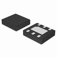
NCP5661MN12T2G ON Semiconductor, NCP5661MN12T2G Datasheet

NCP5661MN12T2G
Specifications of NCP5661MN12T2G
NCP5661MN12T2GOSTR
Available stocks
Related parts for NCP5661MN12T2G
NCP5661MN12T2G Summary of contents
Page 1
NCP5661, NCV5661 Low Output Voltage, Ultra-Fast 1.0 A Low Dropout Linear Regulator with Enable The NCP5661/NCV5661 is a high performance, low dropout linear regulator designed for high power applications that require up to 1.0 A current offered in ...
Page 2
PIN FUNCTION DESCRIPTION Pin Pin Adj/Fixed Adj/Fixed DFN6 DPAK−5 Pin Name 1 1 Enable 2 EPAD 3, TAB Ground out 6 5 Adj (Adjustable Version Error Flag (Fixed Version) MAXIMUM RATINGS ...
Page 3
ELECTRICAL CHARACTERISTICS (V − 1.5 V, for typical values T = 25°C, for min/max values T in out J Characteristic ADJUSTABLE OUTPUT VERSION Input Voltage Output Noise Voltage ( 100 kHz) Output Voltage Accuracy ...
Page 4
ELECTRICAL CHARACTERISTICS (V − 1.5 V, for typical values T = 25°C, for min/max values T in out J Characteristic FIXED OUTPUT VOLTAGE Input Voltage Output Noise Voltage (V = 0.9 V) out Output Voltage Accuracy T = ...
Page 5
V in Voltage Reference Block out ref *C = 5.0 to 200 pF C Figure 1. Typical Schematic, Adjustable Output Version V in Voltage Reference Block C in Figure 2. Typical ...
Page 6
T , JUNCTION TEMPERATURE (°C) J Figure 3. Dropout Voltage vs. Temperature 3.5 3.0 2.5 2.0 1.5 1.0 0.5 0 −40 − ...
Page 7
INPUT−OUTPUT VOLTAGE DIFFERENTIAL (V) Figure 9. Output Current vs. Input−Output Voltage Differential 100 Start: ...
Page 8
1.0 A out TIME (1.0 ms/Div) Figure 15. Load Transient Response The NCP5661 is a high performance low dropout 1.0 A linear regulator suitable for high power applications, featuring an ultra−fast response time and low ...
Page 9
Copper 140 2 oz Copper 100 200 300 400 COPPER AREA (mm Figure 18. DFN6 Thermal Resistance vs. Copper Area Figure 19. Test Board used for Evaluation http://onsemi.com 9 500 ...
Page 10
... ORDERING INFORMATION Device NCP5661DTADJRKG NCP5661DT12RKG NCP5661DT18RKG NCP5661DT33RKG NCV5661DTADJRKG* NCV5661DT12RKG* NCV5661DT18RKG* NCV5661DT33RKG* NCP5661MNADJT2G NCP5661MN12T2G NCP5661MN15T2G NCP5661MN18T2G NCP5661MN25T2G NCP5661MN28T2G NCP5661MN30T2G NCP5661MN33T2G NCV5661MNADJT2G* NCV5661MN12T2G* NCV5661MN15T2G* NCV5661MN18T2G* NCV5661MN25T2G* NCV5661MN28T2G* NCV5661MN30T2G* NCV5661MN33T2G* NOTE: Additional Fix output voltages are available upon request. †For information on tape and reel specifications, including part orientation and tape sizes, please refer to our Tape and Reel Packaging Specifications Brochure, BRD8011/D. *NCV rated devices are subjected to and meet the AECQ− ...
Page 11
... L1 SEATING PLANE SOLDERING FOOTPRINT 2.15 6X (NOTE 3) 0. *For additional information on our Pb−Free strategy and soldering C details, please download the ON Semiconductor Soldering and Mounting Techniques Reference Manual, SOLDERRM/D. http://onsemi.com 11 MILLIMETERS MIN NOM MAX A 0.80 −−− 0.90 0.00 −−− ...
Page 12
... Opportunity/Affirmative Action Employer. This literature is subject to all applicable copyright laws and is not for resale in any manner. PUBLICATION ORDERING INFORMATION LITERATURE FULFILLMENT: Literature Distribution Center for ON Semiconductor P.O. Box 5163, Denver, Colorado 80217 USA Phone: 303−675−2175 or 800−344−3860 Toll Free USA/Canada Fax: 303− ...


