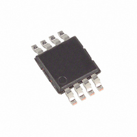
MAX8860EUA27+ Maxim Integrated Products, MAX8860EUA27+ Datasheet - Page 7

MAX8860EUA27+
Manufacturer Part Number
MAX8860EUA27+
Description
IC REG LDO 2.77V/ADJ .3A 8-UMAX
Manufacturer
Maxim Integrated Products
Datasheet
1.MAX8860EUA33.pdf
(8 pages)
Specifications of MAX8860EUA27+
Regulator Topology
Positive Fixed or Adjustable
Voltage - Output
2.77V, 1.25 ~ 6.5 V
Voltage - Input
2.5 ~ 6.5 V
Voltage - Dropout (typical)
0.155V @ 300mA
Number Of Regulators
1
Current - Output
300mA (Min)
Current - Limit (min)
330mA
Operating Temperature
-40°C ~ 85°C
Mounting Type
Surface Mount
Package / Case
8-MSOP, Micro8™, 8-uMAX, 8-uSOP,
Number Of Outputs
1
Polarity
Positive
Input Voltage Max
6.5 V
Output Voltage
2.7 V
Output Type
Fixed
Dropout Voltage (max)
0.22 V at 200 mA
Output Current
300 mA
Line Regulation
0.1 %
Load Regulation
0 %
Voltage Regulation Accuracy
1.4 %
Maximum Power Dissipation
0.33 W
Maximum Operating Temperature
+ 85 C
Mounting Style
SMD/SMT
Minimum Operating Temperature
- 40 C
Lead Free Status / RoHS Status
Lead free / RoHS Compliant
Choose R2 = 100kΩ to optimize power consumption,
accuracy, and high-frequency power-supply rejection.
Ensure that the total current through the external resis-
tive feedback and load resistors is not less than 10µA.
Since the V
set the output using fixed resistors instead of trim pots.
In preset voltage mode, connect SET to GND. Keep
impedances between SET and ground to less than
100kΩ. Otherwise, spurious conditions can cause V
to exceed the 60mV Dual Mode threshold.
Drive SHDN low to place the MAX8860 in shutdown
mode. In shutdown mode, the pass transistor, control
circuit, reference, and all biases are turned off, reduc-
ing the supply current to typically 10nA. Connect SHDN
to IN for normal operation.
The MAX8860 includes short-circuit protection. It includes
a current limiter that controls the pass transistor’s gate
voltage to limit the output current to about 770mA. For
design purposes, the minimum current limit is 330mA.
Thermal overload protection limits total power dissipa-
tion in the MAX8860. When the junction temperature
(T
nal to the shutdown logic, turning off the pass transistor
and allowing the IC to cool. The pass transistor turns on
again after the IC’s junction temperature typically cools
by 20°C, resulting in a pulsed output during continuous
thermal overload conditions.
Thermal overload protection is designed to protect the
MAX8860 against fault conditions. Stressing the device
with high-load currents and high input-output differen-
tial voltages (which result in die temperatures above
+125°C) may cause a momentary overshoot (2% to 8%
for 200ms) when the load is completely removed.
Remedy this by raising the minimum load current from
0 (+125°C) to 100µA (+150°C). This is accomplished
with an external load resistor. For continuous operation,
do not exceed the absolute maximum junction tempera-
ture rating of +150°C.
Maximum power dissipation of the MAX8860 depends
on the thermal resistance of the case and circuit board,
the temperature difference between the die junction
and ambient air, and the rate of air flow. The power dis-
sipated by the device is:
J
) exceeds +170°C, the thermal sensor sends a sig-
SET
tolerance is typically less than ±20mV,
P = I
Thermal Overload Protection
_______________________________________________________________________________________
OUT
(V
Operating Region and
IN
- V
Power Dissipation
OUT
)
Current Limit
Shutdown
SET
Linear Regulator in µMAX
The maximum power dissipation is:
where: T
The MAX8860’s pins perform the dual function of provid-
ing an electrical connection as well as channeling heat
away from the die. Use wide circuit-board traces and
large, solid copper polygons to improve power dissipa-
tion. Using multiple vias to buried ground planes further
enhances thermal conductivity.
The MAX8860 has a unique protection scheme that lim-
its the reverse supply current to less than 1mA when
either V
monitors the polarity of these two pins, disconnecting
the internal circuitry and parasitic diodes when the
applied voltage is reversed. This feature prevents the
device from overheating and damaging an improperly
installed battery.
The MAX8860 uses an external 33nF compensation
capacitor for minimizing load- and line-regulation errors
and for lowering output noise. When the output voltage
shifts due to varying load current or input voltage, the
integrator capacitor voltage is raised or lowered to
compensate for the systematic offset at the error ampli-
fier. Compensation is limited to ±5% to minimize tran-
sient overshoot when the device goes out of dropout,
current limit, or thermal shutdown.
When the output voltage goes out of regulation—such
as during dropout, current limit, or thermal shutdown—
FAULT goes low. In addition, the fault-detection circuitry
detects when the input-to-output voltage differential is
insufficient to ensure good load and line regulation at
the output. When the input-to-output voltage differential
is less than 130mV for a load current of 200mA, FAULT
also goes low. The differential threshold is designed to
be always higher than and track with the dropout volt-
age, and to scale proportionally with load current (see
Fault Detect Threshold vs. Load Current graph in the
Typical Operating Characteristics).
The FAULT pin is an open-drain N-channel MOSFET. To
create a voltage level output, connect a pull-up resistor
from FAULT to OUT. To minimize current consumption,
make this resistor as large as practical. A 100kΩ resistor
works well for most applications.
Low-Dropout, 300mA
T
θ
JMAX
JA
IN
A
is the ambient temperature
= 244°C/W
or V
= +150°C
P
S HDN
MAX
Reverse Battery Protection
= (T
falls below GND. The circuitry
Fault-Detection Circuitry
JMAX
Integrator Circuitry
- T
A
) / θ
JA
7


