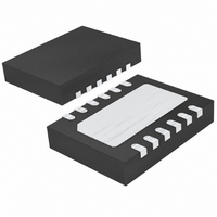
LT4356IDE-1#TRPBF Linear Technology, LT4356IDE-1#TRPBF Datasheet - Page 13

LT4356IDE-1#TRPBF
Manufacturer Part Number
LT4356IDE-1#TRPBF
Description
IC OVERVOLT PROT REG 12-DFN
Manufacturer
Linear Technology
Datasheet
1.LT4356IDE-1TRPBF.pdf
(26 pages)
Specifications of LT4356IDE-1#TRPBF
Voltage - Working
4 ~ 80V
Voltage - Clamping
27V Adj
Technology
Mixed Technology
Number Of Circuits
1
Applications
Automotive
Package / Case
12-DFN
Lead Free Status / RoHS Status
Lead free / RoHS Compliant
Power (watts)
-
Lead Free Status / Rohs Status
Compliant
Available stocks
Company
Part Number
Manufacturer
Quantity
Price
APPLICATIONS INFORMATION
This fi xed early warning period allows the systems to per-
form necessary backup or house-keeping functions before
the power supply is cut off. After V
threshold, the pass transistor turns off immediately. Note
that during an overcurrent event, the timer current is not
reduced to 5μA after V
since it would lengthen the overall fault timer period and
cause more stress on the power MOSFET.
As soon as the fault condition has disappeared, a 2μA
current starts to discharge the timer capacitor to ground.
When V
pump starts to pull the GATE pin high, turning on the
MOSFET. The TMR pin is then actively regulated to 0.5V
until the next fault condition appears. The total cool down
timer period is given by:
MOSFET Selection
The LT4356 drives an N-channel MOSFET to conduct the
load current. The important features of the MOSFET are
on-resistance R
V
The maximum allowable drain-source voltage must be
higher than the supply voltage. If the output is shorted
to ground or during an overvoltage event, the full supply
voltage will appear across the MOSFET.
The gate drive for the MOSFET is guaranteed to be more
than 10V and less than 16V for those applications with V
higher than 8V. This allows the use of standard threshold
(BR)DSS
t
COOL
TMR
, the threshold voltage, and the SOA.
=
reaches the 0.5V threshold, the internal charge
C
TMR
DS(ON)
2μA
• 0.85V
, the maximum drain-source voltage
TMR
has reached 1.25V threshold,
V
IN
TMR
crosses the 1.35V
Figure 3. Prototypical Transient Waveform
t
r
V
PK
τ
CC
voltage N-channel MOSFETs. For systems with V
than 8V, a logic level MOSFET is required since the gate
drive can be as low as 4.5V.
The SOA of the MOSFET must encompass all fault condi-
tions. In normal operation the pass transistor is fully on,
dissipating very little power. But during either overvoltage
or overcurrent faults, the GATE pin is servoed to regu-
late either the output voltage or the current through the
MOSFET. Large current and high voltage drop across the
MOSFET can coexist in these cases. The SOA curves of
the MOSFET must be considered carefully along with the
selection of the fault timer capacitor.
Transient Stress in the MOSFET
During an overvoltage event, the LT4356 drives a series
pass MOSFET to regulate the output voltage at an acceptable
level. The load circuitry may continue operating throughout
this interval, but only at the expense of dissipation in the
MOSFET pass device. MOSFET dissipation or stress is a
function of the input voltage waveform, regulation voltage
and load current. The MOSFET must be sized to survive
this stress.
Most transient event specifi cations use the model shown
in Figure 3. The idealized waveform comprises a linear
ramp of rise time t
exponentially decaying back to V
of t. A common automotive transient specifi cation has
constants of t
condition known as “load dump” has constants of t
5ms, V
PK
= 60V and τ = 200ms.
r
= 10μs, V
r
, reaching a peak voltage of V
LT4356-1/LT4356-2
4356 F03
PK
= 80V and τ = 1ms. A surge
IN
with a time constant
13
CC
PK
4356fa
less
and
r
=


