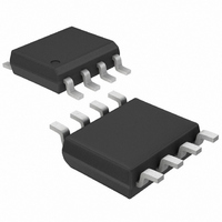
MAX882CSA Maxim Integrated Products, MAX882CSA Datasheet - Page 4

MAX882CSA
Manufacturer Part Number
MAX882CSA
Description
IC REG LINEAR LDO 3.3V/ADJ 8SOIC
Manufacturer
Maxim Integrated Products
Datasheet
1.MAX882CSA.pdf
(17 pages)
Specifications of MAX882CSA
Regulator Topology
Positive Fixed or Adjustable
Voltage - Output
3.3V, 1.25 ~ 11 V
Voltage - Input
2.7 ~ 11.5 V
Voltage - Dropout (typical)
0.32V @ 200mA
Number Of Regulators
1
Current - Output
200mA
Operating Temperature
0°C ~ 70°C
Mounting Type
Surface Mount
Package / Case
8-SOIC (3.9mm Width)
Lead Free Status / RoHS Status
Contains lead / RoHS non-compliant
Current - Limit (min)
-
Other names
154784
Q1154784
Q1154784
Available stocks
Company
Part Number
Manufacturer
Quantity
Price
Company:
Part Number:
MAX882CSA
Manufacturer:
MAXIM
Quantity:
7
Part Number:
MAX882CSA
Manufacturer:
MAXIM/美信
Quantity:
20 000
Company:
Part Number:
MAX882CSA-T
Manufacturer:
LT
Quantity:
3 818
Part Number:
MAX882CSA-T
Manufacturer:
MAXIM/美信
Quantity:
20 000
5V/3.3V or Adjustable, Low-Dropout,
Low I
ELECTRICAL CHARACTERISTICS (continued)
(V
+85°C, unless otherwise noted. Typical values are at T
Note 1: Electrical specifications are measured by pulse testing and are guaranteed for a junction temperature (T
Note 2: (V
Note 3: Dropout Voltage is (V
Note 4: Since standby mode inhibits the output but keeps all biasing circuitry alive, the Standby Quiescent Current is similar to the
Note 5: Foldback Current Limit was characterized by pulse testing to remain below the maximum junction temperature (not
Note 6: The Reverse-Current Protection Threshold is the output/input differential voltage (V
Note 7: Noise is tested using a bandpass amplifier with two poles at 10Hz and two poles at 10kHz.
4
STBY Threshold Voltage
STBY Hysteresis
STBY Input Leakage Current
OFF Threshold Voltage
OFF Input Leakage Current
Output Noise
IN
_______________________________________________________________________________________
= 6V (MAX883) or V
ing temperature range, unless otherwise noted. Specifications to -40°C are guaranteed by design and not production tested.
Figure 5. Therefore, the combination of high output current and high supply voltage is not tested.
MAX883 is tested by measuring the V
The difference (V
normal operating quiescent current.
production tested).
protection switchover occurs and the pass transistor is turned off. See the section Reverse-Current Protection in the Detailed
Description.
IN
PARAMETER
- V
Q
OUT
, 200mA Linear Regulators
) is limited to keep the product (I
IN
IN
- V
= 4.3V (MAX882/MAX884), C
IN
OUT
- V
) is then measured and defined as ∆V
OUT
SYMBOL
∆V
) when V
V
V
V
I
IH OFF
IL OFF
I
STBY
OFF
STBY
e
STBY
n
OUT
OUT
STBY signal falling, MAX882_A
MAX882_A
V
In off mode, MAX883_A, MAX884_A
In on mode, SET = OUT, V
MAX883_A, MAX884_A
In on mode, SET = OUT, 6V < V
MAX883_A, MAX884_A
10Hz to 10kHz, SET = OUT, R
C
at V
V
OUT
STBY
OUT
falls to 100mV below its nominal value at V
OFF
IN
J
= 2.2µF (Note 7)
= +25°C.) (Note 1)
x (V
= V
= 7V, then V
= V
OUT
IN
IN
IN
or 0
- V
or 0, MAX882_A
= 2.2µF, STBY or OFF = V
CONDITIONS
OUT
IN
)) from exceeding the package power dissipation limits. See
is lowered until V
DO
.
IN
< 6V,
L
= 1kΩ,
IN
< 11.5V,
OUT
OUT
IN
, SET = GND, LBI = V
falls 100mV below the measured value.
IN
- V
= (V
MIN
1.15
IN
2.0
3.0
) at which reverse-current
OUT
+ 2V). For example, the
±0.01
±0.01
TYP
1.20
250
7
J
) within the operat-
IN
MAX
1.25
±50
±50
0.4
, T
J
= -40°C to
UNITS
µV
mV
nA
nA
V
V
RMS


