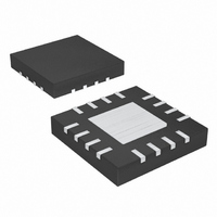
MAX5086BATE+T Maxim Integrated Products, MAX5086BATE+T Datasheet - Page 9

MAX5086BATE+T
Manufacturer Part Number
MAX5086BATE+T
Description
IC REG LINEAR 5V/ADJ 16-TQFN
Manufacturer
Maxim Integrated Products
Datasheet
1.MAX5086BATE.pdf
(13 pages)
Specifications of MAX5086BATE+T
Regulator Topology
Positive Fixed or Adjustable
Voltage - Output
5V, 2.5 ~ 11 V
Voltage - Input
6.5 ~ 45 V
Voltage - Dropout (typical)
0.9V @ 250mA
Number Of Regulators
1
Current - Output
250mA (Min)
Operating Temperature
-40°C ~ 125°C
Mounting Type
Surface Mount
Package / Case
16-TQFN Exposed Pad
Polarity
Positive
Number Of Outputs
1
Output Type
Adjustable, Fixed
Output Voltage
2.5 V to 11 V, 5 V
Output Current
0.25 A
Line Regulation
1 mV / V
Load Regulation
0.045 Ohms
Dropout Voltage (max)
2.2 V
Input Voltage Max
65 V
Maximum Operating Temperature
+ 125 C
Minimum Operating Temperature
- 40 C
Maximum Power Dissipation
2666 mW
Mounting Style
SMD/SMT
Reference Voltage
1.235 V
Lead Free Status / RoHS Status
Lead free / RoHS Compliant
Current - Limit (min)
-
Lead Free Status / Rohs Status
Lead free / RoHS Compliant
The MAX5086 features dual-mode operation, in either a
preset voltage mode or an adjustable mode. In preset
voltage mode, internal feedback resistors set the
MAX5086’s output voltage to +3.3V or +5V. Select pre-
set voltage mode by connecting SET to ground. In
adjustable mode, select an output between +2.5V and
+11V using two external resistors connected as a volt-
age-divider to SET (Figure 2). Set the output voltage
using the following equation:
where V
mately 100kΩ.
The MAX5086 high-voltage regulator provides up to
250mA of output current. The input voltage extends to
+45V. Package power dissipation limits the amount of
output current available for a given input/output voltage
and ambient temperature. Figure 3 depicts the maxi-
mum power dissipation curve for these devices. The
graph assumes that the exposed pad of the MAX5086
package is set up per JEDEC specifications.
Use Figure 3 to determine the allowable package dissi-
pation (P
Alternately, use the following formula to calculate the
allowable package dissipation:
After determining the allowable package dissipation
calculate the maximum output current using the follow-
ing formula:
The above equations do not include the negligible
power dissipation from self-heating due to the IC
ground current.
P
D
Linear Regulator with Adjustable Reset Delay
=
Available Output Current Calculation
SET
I
OUT(MAX)
⎧
⎪
⎪
⎨
⎪
⎪
⎩
D
2 666
2 666
For
.
.
= 1.23V and R2 is chosen to be approxi-
) for a given ambient temperature.
V
+
Applications Information
OUT
W for T
W
70
_______________________________________________________________________________________
°
−
≅
C
0 0333
=
V
Output Voltage Selection
<
.
IN
A
V
T
SET
−
P
A
≤ +
D
V
45V, 250mA, Low-Quiescent-Current
°
OUT
W
≤ +
C
x
70
x T
⎛
⎜
⎝
125
°
1
C
(
≤
+
A
°
C
250mA
R
R
−
1
2
70
⎞
⎟
⎠
°
C
)
⎫
⎪
⎪
⎬
⎪
⎪
⎭
Example 1:
T
V
V
Find the maximum allowable output current. First calcu-
late package dissipation at the given temperature as
follows:
Then determine the maximum output current:
Figure 3. Calculated Maximum Power Dissipation vs.
Temperature
A
IN
OUT
P
D
= +85°C
= +14V
=
= +5V
2
I
OUT(MAX)
.
666
4.0
3.5
3.0
2.5
2.0
1.5
1.0
0.5
0
W
0
2.666W
−
MAXIMUM POWER DISSIPATION
20
0
.
=
0333
40
vs. TEMPERATURE
TEMPERATURE (°C)
(14V) (5V)
(2.1665W)
60
°
DERATE
33.3mW/°C
W
C
−
(85 C
80
°
100
−
=
120
70 C)
271mA
°
140
=
2
.
1665
W
9


