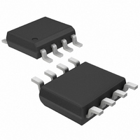
MAX1659ESA+T Maxim Integrated Products, MAX1659ESA+T Datasheet - Page 9

MAX1659ESA+T
Manufacturer Part Number
MAX1659ESA+T
Description
IC LDO REG 350MA 16.5VIN 8-SOIC
Manufacturer
Maxim Integrated Products
Datasheet
1.MAX1658ESA.pdf
(12 pages)
Specifications of MAX1659ESA+T
Regulator Topology
Positive Fixed or Adjustable
Voltage - Output
5V, 1.25 ~ 16 V
Voltage - Input
2.7 ~ 16.5 V
Voltage - Dropout (typical)
0.49V @ 350mA
Number Of Regulators
1
Current - Output
350mA (Min)
Operating Temperature
-40°C ~ 85°C
Mounting Type
Surface Mount
Package / Case
8-SOIC (3.9mm Width)
Number Of Outputs
1
Polarity
Positive
Input Voltage Max
16.5 V
Output Voltage
1.25 V to 16 V, 5 V
Output Type
Adjustable, Fixed
Dropout Voltage (max)
0.875 V at 350 mA
Output Current
350 mA
Line Regulation
0.05 % / V
Load Regulation
0.003 % / mA
Voltage Regulation Accuracy
3 %
Maximum Power Dissipation
1.2 W
Maximum Operating Temperature
+ 85 C
Mounting Style
SMD/SMT
Minimum Operating Temperature
- 40 C
Reference Voltage
1.246 V
Lead Free Status / RoHS Status
Lead free / RoHS Compliant
Current - Limit (min)
-
Lead Free Status / Rohs Status
Lead free / RoHS Compliant
To maintain stability, connect a ≥10µF capacitor with
less than 200mΩ equivalent series resistance (ESR)
from OUT to GND. Larger output capacitors improve
load-transient response. Currents lower than 350mA
make the use of smaller output capacitors possible.
Table 1 shows the maximum output current typically
achieved using various output capacitors. Output volt-
ages higher than 3.3V require less output capacitance
to remain stable.
Table 1. Typical Load Current Capabilities
__________Applications Information
Output Capacitor Selection and Stability
OUTPUT CAPACITOR
2.2µF tantalum
4.7µF tantalum
10µF tantalum
_______________________________________________________________________________________
LOAD CURRENT RANGE
0mA to 120mA
0mA to 250mA
0mA to 350mA
Low-Dropout Linear Regulators
The use of a 0.1µF to 10µF input bypass capacitor is
recommended. Larger capacitors provide better sup-
ply-noise rejection and line-transient response, as well
as improved performance when the supply has a high
AC impedance. Polarized input bypass capacitors will
be damaged under reverse battery conditions. If
reverse input voltages are expected, use a non-polar-
ized capacitor at the input.
The MAX1658/MAX1659 exhibit 2.5mVp-p of noise dur-
ing normal operation. This noise level is negligible in
most applications.
The MAX1658/MAX1659 are designed to maintain
excellent power-supply rejection (55dB) at 50Hz/60Hz
(or 50dB at 120Hz). These regulators are ideal for wall-
cube applications that may contain significant ripple.
Larger input and output capacitors will further improve
the circuit’s AC response. See the Power-Supply
Rejection Ratio vs. Frequency graphs in the Typical
Operating Characteristics.
TRANSISTOR COUNT: 207
___________________Chip Information
350mA, 16.5V Input,
Input Bypass Capacitor
Noise and PSRR
9


