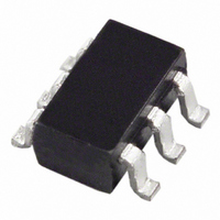
ADP3307ART-2.75-RL Analog Devices Inc, ADP3307ART-2.75-RL Datasheet - Page 7

ADP3307ART-2.75-RL
Manufacturer Part Number
ADP3307ART-2.75-RL
Description
IC REG LDO 2.75V 100MA SOT-23-6
Manufacturer
Analog Devices Inc
Series
anyCAP®r
Datasheet
1.ADP3307ART-2.7-RL.pdf
(8 pages)
Specifications of ADP3307ART-2.75-RL
Rohs Status
RoHS non-compliant
Regulator Topology
Positive Fixed
Voltage - Output
2.75V
Voltage - Input
3 ~ 12 V
Voltage - Dropout (typical)
0.126V @ 100mA
Number Of Regulators
1
Current - Output
100mA
Operating Temperature
-25°C ~ 85°C
Mounting Type
Surface Mount
Package / Case
SOT-23-6
Current - Limit (min)
-
Other names
ADP3307ART-2.75RL
Thermal Overload Protection
The ADP3307 is protected against damage due to excessive
power dissipation by its thermal overload protection circuit,
which limits the die temperature to a maximum of 165°C.
Under extreme conditions (i.e., high ambient temperature and
power dissipation), where die temperature starts to rise above
165°C, the output current is reduced until the die temperature
has dropped to a safe level. Output current is restored when the
die temperature is reduced.
Current and thermal limit protections are intended to protect
the device against accidental overload conditions. For normal
operation, device power dissipation should be externally limited
so that junction temperatures will not exceed 125°C.
Calculating Junction Temperature
Device power dissipation is calculated as follows:
Where I
and V
Assuming I
V
With a maximum junction temperature of 125°C, this yields a
maximum ambient temperature of 87°C.
Printed Circuit Board Layout Consideration
Surface mount components rely on the conductive traces or
pads to transfer heat away from the device. Appropriate PC
board layout techniques should be used to remove heat from the
immediate vicinity of the package.
The following general guidelines will be helpful when designing
a board layout:
1. PC board traces with larger cross section areas will remove
2. Increase the surface area exposed to open air so heat can be
3. Do not use solder mask or silkscreen on the heat dissipating
OUT
more heat. For optimum results, use PC boards with thicker
copper and wider traces.
removed by convection or forced air flow.
traces because it will increase the junction-to-ambient ther-
mal resistance of the package.
V
OUT
= 3.3 V, device power dissipation is:
IN
LOAD
1 F
∆T = T
C1
P
are input and output voltages respectively.
D
LOAD
+
= (5.5 – 3.3) 0.1 + 5.5 × 2 mA = 0.231 W
and I
P
D
= 100 mA, I
J
= (V
– T
ADP3307-3.3
IN
GND
SD
OFF
A
IN
are load current and ground current, V
= P
– V
ON
GND
OUT
ERR
D
NR
OUT
× θ
GND
) I
JA
R1
= 2 mA, V
LOAD
= 0.231 × 165 = 38°C
330k
C
10nF
NR
E
+ (V
OUT
+
IN
IN
C2
4.7 F
) I
= 5.5 V and
GND
V
OUT
= 3.3V
IN
Shutdown Mode
Applying a high signal to the shutdown pin or tying it to the
input pin will turn the output ON. Pulling the shutdown pin
down to a low level or tying it to ground will turn the output
OFF. In shutdown mode, quiescent current is reduced to less
than 1 µA.
Error Flag Dropout Detector
The ADP3307 will maintain its output voltage over a wide
range of load, input voltage and temperature conditions. If the
output is about to lose regulation, for example, by reducing the
supply voltage below the combined regulated output and drop-
out voltages, the ERR pin will be activated. The ERR output is
an open collector that will be driven low.
Once set, the ERRor flag’s hysteresis will keep the output low
until a small margin of operating range is restored either by
raising the supply voltage or reducing the load.
APPLICATIONS CIRCUITS
Crossover Switch
The circuit in Figure 4 shows that two ADP3307s can be used
to form a mixed supply voltage system. The output switches
between two different levels selected by an external digital input.
Output voltages can be any combination of voltages from the
Ordering Guide of the data sheet.
Higher Output Current
The ADP3307 can source up to 100 mA without any heatsink
or pass transistor. If higher current is needed, an appropriate
pass transistor can be used, as in Figure 5, to increase the out-
put current to 1 A.
V
IN
V
IN
= 4V TO 12V
OUTPUT SELECT
= 4V TO 8V
5V
0V
47 F
1.0 F
C1
C1
AAVID531002 HEAT SINK IS USED
+
IN
SD
IN
SD
50
ADP3307-2.7
ADP3307-3.3
SD
R1
ADP3307-3.3
MJE253
GND
GND
GND
IN
OUT
OUT
ERR
OUT
+
+
C2
0.47 F
C2
10 F
ADP3307
V
OUT
V
OUT
= 3.3V@1A
= 2.7V/3.3V


