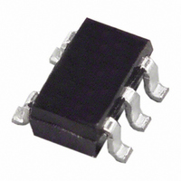
ADP3309ART-3.3-RL7 Analog Devices Inc, ADP3309ART-3.3-RL7 Datasheet

ADP3309ART-3.3-RL7
Specifications of ADP3309ART-3.3-RL7
Available stocks
Related parts for ADP3309ART-3.3-RL7
ADP3309ART-3.3-RL7 Summary of contents
Page 1
FEATURES ±1.2% accuracy over line and load regulations @ 25°C Ultralow dropout voltage: 120 mV typical @ 100 mA Requires only C = 0.47 μF for stability OUT anyCAP LDOs are stable with all types of capacitors (including MLCC) Current ...
Page 2
ADP3309 TABLE OF CONTENTS Features .............................................................................................. 1 Applications....................................................................................... 1 Functional Block Diagram .............................................................. 1 General Description ......................................................................... 1 Revision History ............................................................................... 2 Specifications..................................................................................... 3 Absolute Maximum Ratings............................................................ 4 ESD Caution.................................................................................. 4 Pin Configuration and Function Descriptions............................. 5 Typical Performance Characteristics ...
Page 3
SPECIFICATIONS @ T = −20°C to +85° 0.47 μ options. Table 1. Parameter Output Voltage Accuracy Line Regulation Load Regulation Ground Current Ground Current in Dropout Dropout Voltage Shutdown Threshold ...
Page 4
ADP3309 ABSOLUTE MAXIMUM RATINGS Table 2. Parameter Input Supply Voltage Shutdown Input Voltage Power Dissipation Operating Ambient Temperature Range Operating Junction Temperature Range θ JA θ JC Storage Temperature Range Lead Temperature (Soldering 10 sec) Vapor Phase (60 sec) Infrared ...
Page 5
PIN CONFIGURATION AND FUNCTION DESCRIPTIONS Table 3. Pin Function Descriptions Pin No. Mnemonic Description 1 IN Regulator Input. 2 GND Ground Pin Active Low Shutdown Pin. Connect to ground to disable the regulator output. When shutdown is not ...
Page 6
ADP3309 TYPICAL PERFORMANCE CHARACTERISTICS 3.302 I = 0mA L 3.301 I = 10mA L 3.300 3.299 I = 50mA 3.298 L 3.297 3.296 I = 100mA L 3.295 3 INPUT VOLTAGE (V) Figure 4. ...
Page 7
OUTPUT LOAD (mA) Figure 10. Dropout Voltage vs. Output Current 5 V OUT INPUT VOLTAGE (V) ...
Page 8
ADP3309 3. 3.3V OUT C = 4.7µF L 3.31 3.30 3.29 3.28 I OUT 100 10 0 100 200 300 TIME (µs) Figure 16. Load Transient 300 I OUT 200 100 3.3V OUT 2 ...
Page 9
THEORY OF OPERATION The ADP3309 anyCAP LDO uses a single control loop for regulation and reference functions. The output voltage is sensed by a resistive voltage divider consisting of R1 and R2, which is varied to provide the available output ...
Page 10
ADP3309 APPLICATION INFORMATION CAPACITOR SELECTION: anyCAP Output Capacitors: As with any micropower device, output transient response is a function of the output capacitance. The ADP3309 is stable with a wide range of capacitor values, types, and ESR (anyCAP). A capacitor ...
Page 11
APPLICATION CIRCUITS CROSSOVER SWITCH The circuit in Figure 23 shows that two ADP3309s can be used to form a mixed supply voltage system. The output switches between two different levels selected by an external digital input. Output voltages can be ...
Page 12
... ADP3309ART-3-REEL −20°C to +85°C ADP3309ART-3-REEL7 −20°C to +85°C 1 ADP3309ARTZ-3REEL7 −20°C to +85°C ADP3309ART-3.3-RL −20°C to +85°C ADP3309ART-3.3-RL7 −20°C to +85°C 1 ADP3309ARTZ-3.3-R7 −20°C to +85°C ADP3309ART-3.6-RL −20°C to +85°C ADP3309ART-3.6-RL7 −20°C to +85°C 1 ADP3309ARTZ-3.6-R7 − ...


