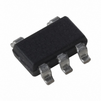
MIC5248-1.2BM5 TR Micrel Inc, MIC5248-1.2BM5 TR Datasheet - Page 7

MIC5248-1.2BM5 TR
Manufacturer Part Number
MIC5248-1.2BM5 TR
Description
IC REG LDO 150MA 1.2V SOT23-5
Manufacturer
Micrel Inc
Datasheet
1.MIC5248-1.2YM5_TR.pdf
(10 pages)
Specifications of MIC5248-1.2BM5 TR
Regulator Topology
Positive Fixed
Voltage - Output
1.2V
Voltage - Input
2.7 ~ 6 V
Number Of Regulators
1
Current - Output
150mA
Current - Limit (min)
160mA
Operating Temperature
-40°C ~ 125°C
Mounting Type
Surface Mount
Package / Case
SOT-23-5, SC-74A, SOT-25
Lead Free Status / RoHS Status
Contains lead / RoHS non-compliant
Voltage - Dropout (typical)
-
Other names
MIC5248-1.2BM5TR
MIC5248-1.2BM5TR
MIC5248-1.2BM5TR
Application Information
Enable/Shutdown
The MIC5248 comes with an active-high enable pin that
allows the regulator to be disabled. Forcing the enable
pin low disables the regulator and sends it into a “zero”
off-mode-current state. In this state, current consumed
by the regulator goes nearly to zero. Forcing the enable
pin high enables the output voltage. This part is CMOS
and the enable pin cannot be left floating; a floating
enable pin may cause an indeterminate state on the
output.
Input Capacitor
An input capacitor is not required for stability. A 1µF
input capacitor is recommended when the bulk ac supply
capacitance is more than 10 inches away from the
device, or when the supply is a battery.
Output Capacitor
The MIC5248 requires an output capacitor for stability.
The design requires 1µF or greater on the output to
maintain stability. The capacitor can be a low-ESR
ceramic chip capacitor. The MIC5248 has been
designed to work specifically with the low-cost, small
chip capacitors. Tantalum capacitors can also be used
for improved capacitance overtemperature. The value of
the capacitor can be increased without bound.
X7R dielectric ceramic capacitors are recommended
because of their temperature performance. X7R-type
capacitors change capacitance by 15% over their
operating temperature range and are the most stable
type of ceramic capacitors. Z5U and Y5V dielectric
capacitors change value by as much 50% and 60%
respectively over their operating temperature ranges. To
use a ceramic chip capacitor with Y5V dielectric, the
value must be much higher than an X7R ceramic or a
tantalum capacitor to ensure the same minimum
capacitance value over the operating temperature range.
Tantalum capacitors have a very stable dielectric (10%
over their operating temperature range) and can also be
used with this device.
Power Good
The Power Good output is an open-drain output. It is
designed essentially to work as a power-on reset
generator once the regulated voltage was up and/or a
fault condition. The output of the Power Good drives low
when a fault condition AND an undervoltage detection
occurs. The Power Good output come back up once the
output has reached 96.5% of its nominal value and a
1ms to 5ms delay has passed. See “Timing Diagram.”
The MIC5248’s internal circuit intelligently monitors
overcurrent, overtemperature and dropout conditions
and ORs these outputs together to indicate some fault
condition. This output is fed into an on-board delay
Micrel, Inc.
August 2006
7
circuitry that drives the open drain transistor to indicate a
fault.
Transient Response
The MIC5248 implements a unique output stage to
dramatically improve transient response recovery time.
The output is a totem-pole configuration with a P-
channel MOSFET pass device and an N-channel
MOSFET clamp. The N-channel clamp is a significantly
smaller device that prevents the output voltage from
overshooting when a heavy load is removed. This
feature helps to speed up the transient response by
significantly decreasing transient response recovery time
during the transition from heavy load (100mA) to light
load (100µA).
Active Shutdown
The MIC5248 also features an active shutdown clamp,
which is an N-channel MOSFET that turns on when the
device is disabled. This allows the output capacitor and
load to discharge, de-energizing the load
Thermal Considerations
The MIC5248 is designed to provide 150mA of
continuous current in a very small package. Maximum
power dissipation can be calculated based on the output
current and the voltage drop across the part. To
determine the maximum power dissipation of the
package, use the junction-to-ambient thermal resistance
of the device and the following basic equation:
T
die,125°C, and T
θ
junction-to-ambient thermal resistance for the MIC5248.
The actual power dissipation of the regulator circuit can
be determined using the equation:
Substituting P
conditions that are critical to the application will give the
maximum operating conditions for the regulator circuit.
For example, when operating the MIC5248-1.2BM5 at
50°C with a minimum footprint layout, the maximum
input voltage for a set output current can be determined
as follows:
SOT-23-5 (M5)
JA
J(max)
Package
is layout dependent; Table 1 shows examples of
is the maximum junction temperature of the
P
P
P
D
D(max)
Table 1. SOT-23-5 Thermal Resistance
D(max)
= (V
D(max)
IN
=
Minimum Footprint
=
θ
A
JA
– V
⎛
⎜
⎜
⎝
⎛
⎜
⎝
is the ambient operating temperature.
125
T
Recommended
for P
J(max)
235°C/W
OUT
235
°
θ
C
) I
JA
D
°
−
C/W
OUT
−
and solving for the operating
50
T
A
+ V
°
C
⎞
⎟
⎟
⎠
⎞
⎟
⎠
IN
θ
I
Copper Clad
GND
JA
185°C/W
1” Square
M9999-080106
MIC5248
145°C/W
θ
JC


