LMS1585AISX-ADJ/NOPB National Semiconductor, LMS1585AISX-ADJ/NOPB Datasheet - Page 5
LMS1585AISX-ADJ/NOPB
Manufacturer Part Number
LMS1585AISX-ADJ/NOPB
Description
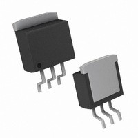
IC REG 5A LDO FAST RESPONS TO263
Manufacturer
National Semiconductor
Datasheet
1.LMS1587CT-3.3.pdf
(8 pages)
Specifications of LMS1585AISX-ADJ/NOPB
Regulator Topology
Positive Adjustable
Voltage - Output
1.25 ~ 5.6 V
Voltage - Input
2.5 ~ 13 V
Voltage - Dropout (typical)
1.2V @ 5A
Number Of Regulators
1
Current - Output
5A
Current - Limit (min)
5A
Operating Temperature
-40°C ~ 125°C
Mounting Type
Surface Mount
Package / Case
TO-263-3, D²Pak (3 leads + Tab), TO-263AA
Lead Free Status / RoHS Status
Lead free / RoHS Compliant
Other names
*LMS1585AISX-ADJ
*LMS1585AISX-ADJ/NOPB
LMS1585AISX-ADJ
*LMS1585AISX-ADJ/NOPB
LMS1585AISX-ADJ
Available stocks
Company
Part Number
Manufacturer
Quantity
Price
Company:

Part Number:
LMS1585AISX-ADJ/NOPB
Manufacturer:
TI
Quantity:
6 000


I
LIMIT
Symbol
Electrical Characteristics
Typicals and limits appearing in normal type apply for T
tion temperature range for operation, 0˚C to 125˚C for commercial grade and −40˚C to 125˚C for industrial grade.
Note 1: Absolute Maximum Ratings indicate limits beyond which damage to the device may occur. Operating Ratings indicate conditions for which the device is
intended to be functional, but specific performance is not guaranteed. For guaranteed specifications and the test conditions, see the Electrical Characteristics.
Note 2: The maximum power dissipation is a function of T
is P
Note 3: For testing purposes, ESD was applied using human body model, 1.5kΩ in series with 100pF.
Note 4: Typical Values represent the most likely parametric norm.
Note 5: All limits are guaranteed by testing or statistical analysis.
Note 6: Load and line regulation are measured at constant junction temperature, and are guaranteed up to the maximum power dissipation of 30W. Power
dissipation is determined by the input/output differential and the output current. Guaranteed maximum power dissipation will not be available over the full input/output
range.
Note 7: The minimum output current required to maintain regulation.
Note 8: I
Note 9: Consult factory for other fixed voltage options.
D
= (T
FULLLOAD
J(max)
Current Limit
Minimum Load
Current (Note 7)
Quiescent Current
Thermal Regulation
Ripple Rejection
Adjust Pin Current
Adjust Pin Current
Temperature Stability
Long Term Stability
RMS Output Noise
(% of V
Thermal Resistance
Junction-to-Case
–T
A
Parameter
is 5A for LMS1585A and 3A for LMS1587.
)/θ
OUT
JA
. All numbers apply for packages soldered directly into a PC board.
)
LMS1585A-ADJ/LMS1585A-3.3/LMS1585A-1.5
V
LMS1587-ADJ/LMS1587-3.3/LMS1587-1.5
V
LMS1585A/87-ADJ
1.5V ≤ V
LMS1585A-3.3/LMS1587-3.3/
LMS1585A-1.5/LMS1587-1.5
V
T
LMS1585A-ADJ
f
I
LMS1585A-1.5
f
I
LMS1585A-3.3
f
I
LMS1587-ADJ
f
C
LMS1587-1.5
f
I
LMS1587-3.3
f
I
10mA ≤ I
1.5V ≤ V
T
10Hz ≤ f ≤ 10kHz
3-Lead TO-263: Control/Output Section
3-Lead TO-220: Control/Output Section
RIPPLE
OUT
RIPPLE
OUT
RIPPLE
OUT
RIPPLE
RIPPLE
OUT
RIPPLE
OUT
A
A
IN
IN
IN
OUT
−V
−V
= 25˚C, 30ms Pulse
= 125˚C, 1000Hrs
= 5V
= 5A, C
= 5A, V
= 5A, V
= 3A, V
= 3A, V
OUT
OUT
= 25µF Tantalum
= 120Hz, V
= 120Hz, C
= 120Hz, C
= 120Hz, V
= 120Hz, C
= 120Hz, C
IN
IN
OUT
(Continued)
= 5.5V
= 5.5V
−V
−V
IN
IN
IN
IN
OUT
OUT
OUT
≤ I
= 4.5V
= 6.3V
= 4.5V
= 6.3V
J(max)
FULLLOAD
= 25µF Tantalum
≤ 5.75V
≤ 5.75V (Note 8)
Conditions
IN
IN
OUT
OUT
OUT
OUT
−V
−V
, θ
J
JA
OUT
= 25µF Tantalum,
= 25µF Tantalum,
OUT
= 25µF Tantalum,
= 25µF Tantalum,
= 25˚C. Limits appearing in Boldface type apply over the entire junc-
, and T
,
= 3V,
= 3V, I
5
A
. The maximum allowable power dissipation at any ambient temperature
OUT
= 3A
(Note 5)
Min
5.0
3.1
60
60
(Note 4)
0.003
0.003
0.03
Typ
6.6
4.3
2.0
7.0
0.2
0.5
72
72
72
72
72
72
55
(Note 5)
0.65/2.7
0.65/2.7
Max
10.0
13.0
120
www.national.com
Units
˚C/W
˚C/W
%/W
mA
mA
dB
dB
dB
dB
dB
dB
µA
µA
%
%
%
A
A
Related parts for LMS1585AISX-ADJ/NOPB
Image
Part Number
Description
Manufacturer
Datasheet
Request
R

Part Number:
Description:
Manufacturer:
National Semiconductor
Datasheet:

Part Number:
Description:
IC REG 5A LDO FAST RESPONS TO263
Manufacturer:
National Semiconductor
Datasheet:
Part Number:
Description:
IC REG LDO FAST 1.5V 5A TO263-3
Manufacturer:
National Semiconductor
Datasheet:
Part Number:
Description:
National Semiconductor [8-Bit D/A Converter]
Manufacturer:
National Semiconductor
Datasheet:
Part Number:
Description:
National Semiconductor [Media Coprocessor]
Manufacturer:
National Semiconductor
Datasheet:
Part Number:
Description:
Digitally Controlled Tone and Volume Circuit with Stereo Audio Power Amplifier, Microphone Preamp Stage and National 3D Sound
Manufacturer:
National Semiconductor
Datasheet:
Part Number:
Description:
Digitally Controlled Tone and Volume Circuit with Stereo Audio Power Amplifier, Microphone Preamp Stage and National 3D Sound
Manufacturer:
National Semiconductor
Datasheet:
Part Number:
Description:
AC97 Rev 2 Codec with Sample Rate Conversion and National 3D Sound
Manufacturer:
National Semiconductor
Part Number:
Description:
Manufacturer:
National Semiconductor
Datasheet:
Part Number:
Description:
Manufacturer:
National Semiconductor
Datasheet:
Part Number:
Description:
General Purpose, Low Voltage, Low Power, Rail-to-Rail Output Operational Amplifiers
Manufacturer:
National Semiconductor
Datasheet:
Part Number:
Description:
8-bit 20 MSPS flash A/D converter.
Manufacturer:
National Semiconductor
Datasheet:
Part Number:
Description:
Low Noise Quad Operational Amplifier
Manufacturer:
National Semiconductor
Datasheet:
Part Number:
Description:
Quad Differential Line Receivers
Manufacturer:
National Semiconductor
Datasheet: