MC7812ACD2T ON Semiconductor, MC7812ACD2T Datasheet - Page 4
MC7812ACD2T
Manufacturer Part Number
MC7812ACD2T
Description
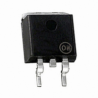
IC REG VOLT POS 1A 12V D2PAK-3
Manufacturer
ON Semiconductor
Datasheet
1.MC7805BDTRKG.pdf
(33 pages)
Specifications of MC7812ACD2T
Regulator Topology
Positive Fixed
Voltage - Output
12V
Voltage - Input
Up to 35V
Voltage - Dropout (typical)
2V @ 1A
Number Of Regulators
1
Current - Output
1A
Operating Temperature
0°C ~ 125°C
Mounting Type
Surface Mount
Package / Case
TO-263-2, D⊃2Pak (2 leads + Tab), TO-263AB
Polarity
Positive
Number Of Outputs
1
Output Type
Fixed
Output Voltage
12 V
Output Current
2.2 A
Line Regulation
120 mV
Load Regulation
25 mV
Input Voltage Max
35 V
Maximum Operating Temperature
+ 125 C
Minimum Operating Temperature
0 C
Mounting Style
SMD/SMT
Voltage Regulation Accuracy
2 %
Lead Free Status / RoHS Status
Contains lead / RoHS non-compliant
Current - Limit (min)
-
Lead Free Status / Rohs Status
Lead free / RoHS Compliant
Other names
MC7812ACD2TOS
Available stocks
Company
Part Number
Manufacturer
Quantity
Price

Part Number:
MC7812ACD2TG
Manufacturer:
ON/安森美
Quantity:
20 000
Company:
Part Number:
MC7812ACD2TR4G
Manufacturer:
ST
Quantity:
30 000
Part Number:
MC7812ACD2TR4G
Manufacturer:
ON/安森美
Quantity:
20 000


3. T
4. Load and line regulation are specified at constant junction temperature. Changes in V
ELECTRICAL CHARACTERISTICS
Output Voltage (T
Output Voltage (5.0 mA ≤ I
Line Regulation (Note 4)
Load Regulation (Note 4)
Quiescent Current
Quiescent Current Change
Ripple Rejection
Dropout Voltage (I
Output Noise Voltage (T
Output Resistance (f = 1.0 kHz)
Short Circuit Current Limit (T
Peak Output Current (T
Average Temperature Coefficient of Output Voltage
separately. Pulse testing with low duty cycle is used.
7.5 Vdc ≤ V
7.5 Vdc ≤ V
8.0 Vdc ≤ V
8.0 Vdc ≤ V
7.3 Vdc ≤ V
5.0 mA ≤ I
5.0 mA ≤ I
250 mA ≤ I
8.0 Vdc ≤ V
7.5 Vdc ≤ V
5.0 mA ≤ I
8.0 Vdc ≤ V
10 Hz ≤ f ≤ 100 kHz
V
low
in
= 35 Vdc
= 0°C for MC78XXC, MC78XXAC,
= *40°C for NCV78XX, MC78XXB, MC78XXAB, and MC78XXAEB
O
O
O
O
in
in
in
in
in
in
in
in
≤ 1.5 A, T
≤ 1.0 A
≤ 1.0 A
≤ 750 mA
≤ 20 Vdc
≤ 25 Vdc, I
≤ 12 Vdc, I
≤ 12 Vdc, I
≤ 20 Vdc, I
≤ 25 Vdc, I
≤ 20 Vdc, T
≤ 18 Vdc, f = 120 Hz, I
J
O
= 25°C)
= 1.0 A, T
J
A
= 25°C)
J
Characteristic
= 25°C)
O
= 25°C
O
O
O
O
O
≤ 1.0 A, P
J
A
= 500 mA
= 1.0 A
= 1.0 A, T
= 1.0 A, T
= 500 mA
= 25°C
J
= 25°C)
= 25°C)
D
O
J
J
≤ 15 W)
= 25°C
= 25°C
= 500 mA
(V
in
= 10 V, I
O
= 1.0 A, T
http://onsemi.com
J
4
= T
Symbol
Reg
V
low
Reg
TCV
I
I
DI
RR
I
V
V
max
V
− V
r
I
SC
B
O
to 125°C (Note 3), unless otherwise noted)
O
O
n
load
line
B
O
O
MC7805AB/MC7805AC/NCV7805AB
Min
O
4.9
4.8
68
−
−
−
−
−
−
−
−
−
−
−
−
−
−
−
−
−
due to heating effects must be taken into account
0.53
0.08
−0.3
Typ
5.0
5.0
0.5
0.8
1.3
4.5
1.3
0.8
3.2
0.3
2.0
0.9
0.2
2.2
83
10
−
Max
5.1
5.2
4.0
6.0
0.8
0.8
0.5
10
12
10
25
25
15
−
−
−
−
−
−
−
mV/°C
mV/V
Unit
Vdc
Vdc
Vdc
mW
mV
mV
mA
mA
dB
A
A
O
Related parts for MC7812ACD2T
Image
Part Number
Description
Manufacturer
Datasheet
Request
R

Part Number:
Description:
ON Semiconductor [VOLTAGE REGULATOR]
Manufacturer:
ON Semiconductor
Datasheet:
Part Number:
Description:
357-036-542-201 CARDEDGE 36POS DL .156 BLK LOPRO
Manufacturer:
ON Semiconductor
Datasheet:
Part Number:
Description:
357-036-542-201 CARDEDGE 36POS DL .156 BLK LOPRO
Manufacturer:
ON Semiconductor
Datasheet:
Part Number:
Description:
357-036-542-201 CARDEDGE 36POS DL .156 BLK LOPRO
Manufacturer:
ON Semiconductor
Datasheet:
Part Number:
Description:
357-036-542-201 CARDEDGE 36POS DL .156 BLK LOPRO
Manufacturer:
ON Semiconductor
Datasheet:
Part Number:
Description:
357-036-542-201 CARDEDGE 36POS DL .156 BLK LOPRO
Manufacturer:
ON Semiconductor
Datasheet:
Part Number:
Description:
357-036-542-201 CARDEDGE 36POS DL .156 BLK LOPRO
Manufacturer:
ON Semiconductor
Datasheet:
Part Number:
Description:
357-036-542-201 CARDEDGE 36POS DL .156 BLK LOPRO
Manufacturer:
ON Semiconductor
Datasheet:
Part Number:
Description:
357-036-542-201 CARDEDGE 36POS DL .156 BLK LOPRO
Manufacturer:
ON Semiconductor
Datasheet:
Part Number:
Description:
357-036-542-201 CARDEDGE 36POS DL .156 BLK LOPRO
Manufacturer:
ON Semiconductor
Datasheet:
Part Number:
Description:
357-036-542-201 CARDEDGE 36POS DL .156 BLK LOPRO
Manufacturer:
ON Semiconductor
Datasheet:
Part Number:
Description:
Manufacturer:
ON Semiconductor
Datasheet:
Part Number:
Description:
Manufacturer:
ON Semiconductor
Datasheet:
Part Number:
Description:
Manufacturer:
ON Semiconductor
Datasheet: