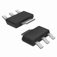
NCP1086ST-33T3G ON Semiconductor, NCP1086ST-33T3G Datasheet - Page 7

NCP1086ST-33T3G
Manufacturer Part Number
NCP1086ST-33T3G
Description
IC REG 1.5A 3.3V SOT223
Manufacturer
ON Semiconductor
Datasheet
1.NCP1086ST-ADJT3.pdf
(13 pages)
Specifications of NCP1086ST-33T3G
Regulator Topology
Positive Fixed
Voltage - Output
3.3V
Voltage - Input
Up to 7V
Voltage - Dropout (typical)
1.05V @ 1.5A
Number Of Regulators
1
Current - Output
1.5A
Current - Limit (min)
1.6A
Operating Temperature
0°C ~ 70°C
Mounting Type
Surface Mount
Package / Case
SOT-223 (3 leads + Tab), SC-73, TO-261
Lead Free Status / RoHS Status
Lead free / RoHS Compliant
Other names
NCP1086ST-33T3GOS
Protection Diodes
regulator it is sometimes necessary to add protection diodes.
If the input voltage of the regulator gets shorted, the output
capacitor will discharge into the output of the regulator. The
discharge current depends on the value of the capacitor, the
output voltage and the rate at which V
NCP1086 series linear regulator, the discharge path is
through a large junction and protection diodes are not
usually needed. If the regulator is used with large values of
output capacitance and the input voltage is instantaneously
shorted to ground, damage can occur. In this case, a diode
connected as shown in Figure 17 or Figure 18 is
recommended.
Output Voltage Sensing
possible to provide true remote load sensing. Load
regulation is limited by the resistance of the conductors
connecting the regulator to the load.
connected as shown in Figure 19.
Figure 17. Protection Diode Scheme for Large Output
Figure 18. Protection Diode Scheme for Large Output
V
V
When large external capacitors are used with a linear
Since the NCP1086 is a three terminal regulator, it is not
For best results the fixed output regulator should be
IN
IN
C
C
1
1
Capacitors (3.3 V Fixed Output)
Capacitors (Adjustable Output)
V
V
IN
IN
IN4002 (optional)
IN4002 (optional)
NCP1086
NCP1086
GND
Adj
V
V
OUT
OUT
R
R
IN
1
2
drops. In the
C
C
2
2
V
V
http://onsemi.com
OUT
OUT
7
V
occurs when R1 is connected directly to the output pin of the
regulator as shown in Figure 20. If R1 is connected to the
load, R
resistance between the regulator and the load becomes
where R
V
Calculating Power Dissipation and
Heatsink Requirements
and current limit circuitry to protect the device. High power
regulators such as these usually operate at high junction
temperatures so it is important to calculate the power
dissipation and junction temperatures accurately to ensure
that an adequate heatsink is used.
IN
IN
For the adjustable regulator, the best load regulation
The NCP1086 linear regulator includes thermal shutdown
Figure 19. Conductor Parasitic Resistance Effects
Can Be Minimized with the Above Grounding
C
Adjustable Output Regulator to Minimize
C
is multiplied by the divider ratio and the effective
Figure 20. Grounding Scheme for the
Scheme for Fixed Output Regulators
= conductor parasitic resistance.
V
V
IN
IN
NCP1086
NCP1086
Parasitic Resistance Effects
Adj
R C
V
V
OUT
OUT
R1 ) R2
R1
R
R
1
2
R
R
C
C
Conductor Parasitic
Conductor Parasitic
Resistance
Resistance
R
R
LOAD
LOAD


