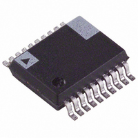
ADG467BRS Analog Devices Inc, ADG467BRS Datasheet - Page 12

ADG467BRS
Manufacturer Part Number
ADG467BRS
Description
IC CHAN PROTECTOR OCTAL 20-SSOP
Manufacturer
Analog Devices Inc
Series
ADG467r
Specifications of ADG467BRS
Rohs Status
RoHS non-compliant
Voltage - Clamping
±40V
Technology
Mixed Technology
Number Of Circuits
8
Applications
General Purpose
Package / Case
20-SSOP
Operating Temperature (min)
-40C
Operating Temperature (max)
85C
Operating Temperature Classification
Industrial
Mounting
Surface Mount
Pin Count
20
Power (watts)
-
Voltage - Working
-
Lead Free Status / RoHS Status
Not Compliant
Available stocks
Company
Part Number
Manufacturer
Quantity
Price
Part Number:
ADG467BRS
Manufacturer:
ADI/亚德诺
Quantity:
20 000
Part Number:
ADG467BRSZ
Manufacturer:
ADI/亚德诺
Quantity:
20 000
Part Number:
ADG467BRSZ-REEL
Manufacturer:
ADI/亚德诺
Quantity:
20 000
ADG467
APPLICATIONS INFORMATION
OVERVOLTAGE AND POWER SUPPLY
SEQUENCING PROTECTION
The ADG467 is ideal for use in applications where input overvol-
tage protection is required and correct power supply sequencing
cannot always be guaranteed. The overvoltage protection ensures
that the output voltage of the channel protector does not exceed the
threshold voltages set by the supplies (see the Circuit Information
section) when there is an overvoltage on the input. When the
input voltage does not exceed these threshold voltages, the channel
protector behaves like a series resistor (62 Ω typical). The resis-
tance of the channel protector does vary slightly with operating
conditions (see the Typical Performance Characteristics
section).
The power sequencing protection is provided by the channel
protector, which becomes a high resistance device when the
supplies to the channel protector are not connected. Under this
condition, all transistors in the channel protector are off and the
only currents that flow are leakage currents, which are at the
microampere level.
–2.5V TO +2.5V
ANALOG IN
Figure 27. Overvoltage and Power Supply Sequencing Protection
LOGIC
LOGIC
LOGIC
LOGIC
LOGIC
LOGIC
LOGIC
GND
+5V
–5V
CONNECTOR
EDGE
Rev. B | Page 12 of 16
V
V
V
V
V
V
V
V
D1
D2
D3
D4
D5
D6
D7
D8
V
ADG467
DD
V
SS
Figure 27 shows a typical application that requires overvoltage
and power supply sequencing protection. The application shows
a hot insertion rack system. This involves plugging a circuit
board or module into a live rack via an edge connector. In this
type of application, it is not possible to guarantee correct power
supply sequencing. Correct power supply sequencing means
that the power supplies should be connected before any external
signals. Incorrect power sequencing can cause a CMOS device
to latch up. This is true of most CMOS devices regardless of the
functionality. RC networks are used on the supplies of the channel
protector (see Figure 27) to ensure that the rest of the circuitry
is powered up before the channel protectors. In this way, the
outputs of the channel protectors are clamped well below V
and V
the supplies on the channel protector never exceed the supply
rails of the board when it is being disconnected. This ensures
that signals on the inputs of the CMOS devices never exceed the
supplies.
V
V
V
V
V
V
V
V
S1
S2
S3
S4
S5
S6
S7
S8
SS
until the capacitors are charged. The diodes ensure that
CONTROL
LOGIC
ADC
DD


