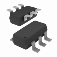
NUP4302MR6T1G ON Semiconductor, NUP4302MR6T1G Datasheet - Page 2

NUP4302MR6T1G
Manufacturer Part Number
NUP4302MR6T1G
Description
IC DIODE ARRAY SCHOTTKY TSOP6
Manufacturer
ON Semiconductor
Datasheet
1.NUP4302MR6T1G.pdf
(4 pages)
Specifications of NUP4302MR6T1G
Voltage - Reverse Standoff (typ)
25V
Voltage - Breakdown
30V
Power (watts)
225mW
Polarization
4 Channel Array - Bidirectional
Mounting Type
Surface Mount
Package / Case
SC-74-6
Applications
General Purpose
Number Of Circuits
4
Voltage - Working
30V
Technology
Diode Array
Product
Schottky Diodes
Peak Reverse Voltage
30 V
Forward Continuous Current
200 mA
Configuration
Octal
Recovery Time
5 ns
Forward Voltage Drop
1 V
Maximum Reverse Leakage Current
30 uA
Maximum Power Dissipation
225 mW
Operating Temperature Range
- 55 C to + 125 C
Mounting Style
SMD/SMT
Lead Free Status / RoHS Status
Lead free / RoHS Compliant
Voltage - Clamping
-
Lead Free Status / Rohs Status
Lead free / RoHS Compliant
Other names
NUP4302MR6T1G
NUP4302MR6T1GOSTR
NUP4302MR6T1GOSTR
Available stocks
Company
Part Number
Manufacturer
Quantity
Price
Company:
Part Number:
NUP4302MR6T1G
Manufacturer:
ON
Quantity:
3 000
Company:
Part Number:
NUP4302MR6T1G
Manufacturer:
ON
Quantity:
30 000
Part Number:
NUP4302MR6T1G
Manufacturer:
ON/安森美
Quantity:
20 000
Stresses exceeding Maximum Ratings may damage the device. Maximum Ratings are stress ratings only. Functional operation above the
Recommended Operating Conditions is not implied. Extended exposure to stresses above the Recommended Operating Conditions may affect
device reliability.
MAXIMUM RATINGS
ELECTRICAL CHARACTERISTICS
Peak Reverse Breakdown Voltage
Forward Power Dissipation (T
Forward Continuous Current
Junction Operating Temperature
Storage Temperature Range
Reverse Breakdown Voltage
Reverse Leakage
Forward Voltage
Forward Voltage
Forward Voltage
Forward Voltage
Total Capacitance
Reverse Recovery Time
+10 V
50 W OUTPUT
GENERATOR
PULSE
Parameter
820 W
0.1 mF
100 mH
2 k
(T
J
= 25°C unless otherwise noted)
Notes: 1. A 2.0 kW variable resistor adjusted for a Forward Current (I
Notes:
Notes:
A
Rating
= 25°C)
Symbol
I
F
V
V
V
V
V
C
I
t
BR
R
2. Input pulse is adjusted so I
3. t
rr
F
F
F
F
T
DUT
p
(T
» t
J
Figure 1. Recovery Time Equivalent Test Circuit
I
V
I
I
I
I
V
V
I
rr
= 25°C unless otherwise noted)
R
F
F
F
F
F
R
R
R
= 0.1 mAdc
= 1.0 mAdc
= 10 mAdc
= 100 mAdc
= I
= 100 mA
= 25 V
= 0 V, f = 1.0 MHz, I/O to Ground
= 0 V, f = 1.0 MHz, I/O to I/O
OSCILLOSCOPE
R
0.1 mF
= 10 mA, I
50 W INPUT
SAMPLING
http://onsemi.com
Conditions
R(REC)
R(peak)
2
= 1.0 mA (Figure 1)
V
R
is equal to 10 mA.
t
INPUT SIGNAL
r
Symbol
10%
V
T
90%
P
T
I
stg
BR
F
F
J
t
p
t
Min
30
−55 to +125
−55 to +150
F
) of 10 mA.
Value
I
I
R
F
225
200
30
(I
Typ
F
= I
at i
OUTPUT PULSE
R
= 10 mA; measured
R(REC)
t
rr
i
R(REC)
Max
0.28
0.35
0.45
1.00
= 1 mA)
5.0
30
28
18
Unit
mW
mA
°C
°C
V
= 1 mA
t
Unit
mA
pF
ns
V
V
V
V
V


