NUS1204MNT1G ON Semiconductor, NUS1204MNT1G Datasheet
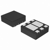
IC OVP W/P-CH MOSFET WDFN6 2X2

NUS1204MNT1G

Manufacturer Part Number
NUS1204MNT1G
Description
IC OVP W/P-CH MOSFET WDFN6 2X2
Manufacturer
ON Semiconductor
Datasheet

Specifications of NUS1204MNT1G

Voltage - Clamping
4.725V
Technology
Mixed Technology
Power (watts)
960mW
Number Of Circuits
1
Applications
General Purpose
Package / Case
6-VDFN Exposed Pad
Number Of Voltages Monitored
1
Monitored Voltage
4.725 V
Overvoltage Threshold
4.725 V
Output Type
PFET Driver
Manual Reset
Not Resettable
Watchdog
No Watchdog
Supply Voltage (max)
12 V
Supply Voltage (min)
0.7 V
Supply Current (typ)
3.9 uA
Maximum Power Dissipation
960 mW
Maximum Operating Temperature
+ 85 C
Mounting Style
SMD/SMT
Minimum Operating Temperature
- 40 C
Lead Free Status / RoHS Status
Lead free / RoHS Compliant
Voltage - Working
-
Lead Free Status / Rohs Status
Lead free / RoHS Compliant

Available stocks

Company
Part Number
Manufacturer
Quantity
Price
Part Number:
NUS1204MNT1G
Manufacturer:
SIRENZA
Quantity:
500
NUS1204MN
Overvoltage Protection IC
with Integrated MOSFET
combining the NCP304 overvoltage protection circuit (OVP) with a
−12 V P−Channel power MOSFET. It is specifically designed to
protect sensitive electronic circuitry from overvoltage transients and
power supply faults. During such hazardous events, the IC quickly
disconnects the input supply from the load, thus protecting the load
before any damage can occur.
adapter or a car accessory charger to power a portable product or
recharge its internal batteries. It has a nominal overvoltage threshold
of 4.725 V which makes it ideal for single cell Li−Ion as well as 3/4
cell NiCD/NiMH applications.
Features
Benefits
Applications
© Semiconductor Components Industries, LLC, 2006
June, 2006 − Rev. 1
This device represents a new level of safety and integration by
The OVP IC is optimized for applications using an external AC−DC
Applications
OvervoltageTurn−Off Time of Less Than 20 ms
Accurate Voltage Threshold of 4.725 V, Nominal
High Accuracy Undervoltage Threshold of 2.0%
−12 V Integrated P−Channel Power MOSFET
Low R
Low Profile 2.0 x 2.0 mm WDFN Package Suitable for Portable
Maximum Solder Reflow Temperature @ 260°C
This device is manufactured with a Pb−Free external lead finish only.
Provide Battery Protection
Integrated Solution Offers Cost and Space Savings
Integrated Solution Improves System Reliability
Portable Computers and PDAs
Cell Phones and Handheld Products
Digital Cameras
DS(on)
= 75 mW @ −4.725 V
†For information on tape and reel specifications,
NUS1204MNT1G
including part orientation and tape sizes, please
refer to our Tape and Reel Packaging Specification
Brochure, BRD8011/D.
GATE
1
GND
OUT
Device
ORDERING INFORMATION
U2 = Specific Device Code
M
G
1
2
3
PIN CONNECTIONS
http://onsemi.com
= Date Code
= Pb−Free Package
CASE 506AN
WDFN6
(Top View)
(Pb−Free)
Package
WDFN6
8
7
Publication Order Number:
3000 Tape & Reel
MARKING
DIAGRAM
1
2
3
NUS1204MN/D
6
5
4
Shipping
U2 M
DRAIN
SOURCE
IN
G
6
5
4

Related parts for NUS1204MNT1G

NUS1204MNT1G Summary of contents

Page 1

... GND (Top View) ORDERING INFORMATION Device Package Shipping NUS1204MNT1G WDFN6 3000 Tape & Reel (Pb−Free) †For information on tape and reel specifications, including part orientation and tape sizes, please refer to our Tape and Reel Packaging Specification Brochure, BRD8011/D. Publication Order Number: NUS1204MN/D ...

Page 2

AC/DC Adapter of Accessory Charger IN PIN FUNCTION DESCRIPTIONS Pin # Symbol 1 GATE Gate pin of the P−Channel Power MOSFET 2 OUT This signal drives the gate of a P−channel Power MOSFET controlled by the voltage level ...

Page 3

MAXIMUM RATINGS (T = 25°C unless otherwise stated) A Rating OUT Voltage to GND Input Pin Voltage to GND Maximum Power Dissipation (Note 1) Thermal Resistance Junction−to−Air (Note 1) Junction Temperature Operating Ambient Temperature Storage Temperature Range ESD Performance (HBM) ...

Page 4

P−CHANNEL MOSFET (T = 25°C, unless otherwise specified) A Parameter Drain to Source On Resistance V = −4 600 −4 1 Zero Gate Voltage Drain Current ...

Page 5

... Opportunity/Affirmative Action Employer. This literature is subject to all applicable copyright laws and is not for resale in any manner. PUBLICATION ORDERING INFORMATION LITERATURE FULFILLMENT: Literature Distribution Center for ON Semiconductor P.O. Box 5163, Denver, Colorado 80217 USA Phone: 303−675−2175 or 800−344−3860 Toll Free USA/Canada Fax: 303− ...

Related keywords