V3.5MLA0805A Littelfuse Inc, V3.5MLA0805A Datasheet - Page 8
V3.5MLA0805A
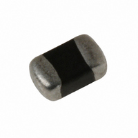
Manufacturer Part Number
V3.5MLA0805A
Description
VARISTR TVS MULTI 3.5V 120A 0805
Manufacturer
Littelfuse Inc
Series
MLr
Specifications of V3.5MLA0805A
Varistor Voltage
7V
Current-surge
120A
Number Of Circuits
1
Maximum Ac Volts
2.5VAC
Maximum Dc Volts
3.5VDC
Energy
0.30J
Package / Case
0805 (2012 Metric)
Suppressor Type
Transient Voltage
Peak Surge Current @ 8/20µs
120A
Varistor Case
0805
Clamping Voltage Vc Max
13V
Peak Energy (10/1000us)
0.3J
Voltage Rating Vdc
3.5V
Voltage Rating Vac
2.5V
Product
MLV
Voltage Rating Dc
3.5 V
Capacitance
2530 pF
Operating Temperature Range
- 55 C to + 125 C
Dimensions
2.01 mm L x 0.50 mm H
Lead Free Status / RoHS Status
Lead free by exemption / RoHS Compliant
Lead Free Status / RoHS Status
Lead free / RoHS Compliant, Lead free by exemption / RoHS Compliant


Multilayer Transient Voltage Surge Suppressors
Soldering Recommendations
Lead (Pb) Soldering Recommendations
The principal techniques used for the soldering of components in surface
mount technology are IR Re-flow & Wave soldering. Typical profiles are
shown in Figures 14 & 15
The termination options available for each solder technique are:
Reflow
1. Nickel Barrier (preferred)
2. Silver/Platinum
The recommended solder for the ML suppressor is a 62/36/2 (Sn/Pb/Ag),
60/40 (Sn/Pb) or 63/37 (Sn/Pb). Littelfuse also recommends an RMA
solder flux.
Wave soldering is the most strenuous of the processes. To avoid the
possibility of generating stresses due to thermal shock, a preheat stage
in
the soldering process is recommended, and the peak temperature of the
solder process should be rigidly controlled.
When using a reflow process, care should be taken to ensure that the
ML chip is not subjected to a thermal gradient steeper than 4 degrees
per second; the ideal gradient being 2 degrees per second. During the
soldering process, preheating to within 100 degrees of the solderís peak
temperature is essential to minimize thermal shock.
Once the soldering process has been completed, it is still necessary to
ensure that any further thermal shocks are avoided. One possible cause
of thermal shock is hot printed circuit boards being removed from the
solder process and subjected to cleaning solvents at room temperature.
The boards must be allowed to cool gradually to less than 50˚C before
cleaning.
Lead-Free (Pb-free) Soldering Recommendations
Littelfuse offers the Nickel-Barrier termination finish for the optimum Pb-
free solder performance.
The preferred solder is 96.5/3.0/0.5 (SnAgCu) with an RMA flux, but
there is a wide selection of pastes & fluxes available with which the nick-
el barrier parts should be compatible.
The reflow profile must be constrained by maximums shown in Figure16.
For Pb-free Wave soldering, Figure 15 still applies.
Note: the Pb-free paste, flux & profile were used for evaluation purposes
by Littelfuse, based upon industry standards & practices. There are
multiple choices of all three available, it is advised that the customer
explores the optimum combination for their process as processes vary
considerably from site to site.
RoHS
176
ML Varistor Series
2. Silver/Palladium
1. Nickel Barrier (preferred)
Wave
w w w . l i t t e l f u s e . c o m
300
250
200
150
100
50
0
0.0
FIGURE 16. LEAD-FREE RE-FLOW SOLDER PROFILE
FIGURE 14. REFLOW SOLDER PROFILE
0.5
FIGURE 15. WAVE SOLDER PROFILE
MAXIMUM TEMPERATURE 260˚C
20 - 40 SECONDS WITHIN 5˚C
PREHEAT ZONE
1.0
FIRST PREHEAT
1.5
TIME (MINUTES)
MAXIMUM WAVE 260
RAMP RATE
<3˚C/s
2.0
SECOND PREHEAT
2.5
230
3.0
5.0
o
60 - 150 SEC
C
> 217˚C
3.5
6.0
4.0
7.0
4.5
Related parts for V3.5MLA0805A
Image
Part Number
Description
Manufacturer
Datasheet
Request
R

Part Number:
Description:
FUSEHOLDER 20A MINI INLINE CRIMP
Manufacturer:
Littelfuse Inc
Datasheet:

Part Number:
Description:
FUSEHOLDER BODY ATO INLINE PNLMT
Manufacturer:
Littelfuse Inc
Datasheet:

Part Number:
Description:
FUSE 2A 63V FAST 1206
Manufacturer:
Littelfuse Inc
Datasheet:
Part Number:
Description:
FUSE 1.25A 63V FAST 1206
Manufacturer:
Littelfuse Inc
Datasheet:
Part Number:
Description:
FUSE .250A 125V FAST 1206
Manufacturer:
Littelfuse Inc
Datasheet:
Part Number:
Description:
FUSE 4A 32V FAST 1206
Manufacturer:
Littelfuse Inc
Datasheet:
Part Number:
Description:
FUSE 1.75A 63V FAST 1206
Manufacturer:
Littelfuse Inc
Datasheet:

Part Number:
Description:
FUSE 1A 32V FST 0603 LEADFREE TR
Manufacturer:
Littelfuse Inc
Datasheet:

Part Number:
Description:
FUSE 1A 32V FAST SLIM 0402
Manufacturer:
Littelfuse Inc
Datasheet:

Part Number:
Description:
FUSE 2A 125V FAST NANO2 SMD
Manufacturer:
Littelfuse Inc
Datasheet:

Part Number:
Description:
FUSE .250A 125V FAST NANO2 SMD
Manufacturer:
Littelfuse Inc
Datasheet:

Part Number:
Description:
FUSE .500A 125V FAST NANO2 SMD
Manufacturer:
Littelfuse Inc
Datasheet:

Part Number:
Description:
FUSE 1.5A 125V FAST NANO2 SMD
Manufacturer:
Littelfuse Inc
Datasheet:

Part Number:
Description:
FUSE 4A 125V FAST NANO2 SMD
Manufacturer:
Littelfuse Inc
Datasheet:

Part Number:
Description:
FUSE 1A 125V FAST NANO2 SMD
Manufacturer:
Littelfuse Inc
Datasheet: