DLP-TXRX-G DLP Design Inc, DLP-TXRX-G Datasheet - Page 3
DLP-TXRX-G
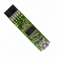
Manufacturer Part Number
DLP-TXRX-G
Description
MODULE USB-TO-TTL SRL UART CONV
Manufacturer
DLP Design Inc
Series
DLP-TXRXr
Datasheet
1.DLP-TXRX-G.pdf
(7 pages)
Specifications of DLP-TXRX-G
Convert From (adapter End)
USB
Convert To (adapter End)
DB9 Female
Features
2 Wires
Interface Type
USB
Operating Supply Voltage
5 V
Product
Interface Modules
For Use With/related Products
Windows® 98 or higher, Mac OS 8.5 or higher
Lead Free Status / RoHS Status
Lead free / RoHS Compliant
Lead Free Status / RoHS Status
Lead free / RoHS Compliant, Lead free / RoHS Compliant
Other names
813-1017


1.3 DTR Open Collector Output
Pin 4 of the DLP-TXRX-G is an open-collector output that is controlled by the DTR#
output of the FT232RL. Upon power up of the DLP-TXRX-G (i.e. when connected to
the host PC), pin 4 is initially driven low via an open-collector transistor until the host
application opens the COM port that the DLP-TXRX-G is assigned to. Once the port is
opened, pin 4 becomes high-impedance. From this point forward, the state of pin 4 can
be changed under software control via the user’s application program by setting and
clearing DTR#.
NOTE: if pin 4 is used to reset an external microcontroller, then upon power up the
processor will not run until the COM port is opened by the host application.
1.4 VCCIO Input
Pin 5 is used to provide power to the I/O pins of the FT232RL in instances where the
external microcontroller/DSP/FPGA/etc is operating at a voltage other than 5 volts. The
acceptable input voltage range on Pin 5 is 1.8 to 5.25 volts. If the external processor is
running at 5.0 volts then Pin 5 can be left disconnected.
If the external processor is running at a voltage other than 5 volts then the solder bridge at
location ‘5’ on the DLP-TXRX-G pcb must be removed and a solder bridge at location
‘3’ must be applied in order for the voltage applied to pin 5 to be used.
Rev 1.4 (Oct 2008)
3
DLP-TXRX DLP Design, Inc.
Related parts for DLP-TXRX-G
Image
Part Number
Description
Manufacturer
Datasheet
Request
R

Part Number:
Description:
KIT DEV DLP LIGHTCOMANDER
Manufacturer:
Logic
Datasheet:

Part Number:
Description:
MODULE DATA-ACQUISITION 8-CH
Manufacturer:
DLP Design Inc
Datasheet:

Part Number:
Description:
MODULE DATA-ACQUISITION 20-CH
Manufacturer:
DLP Design Inc
Datasheet:

Part Number:
Description:
RFID READER/WRITER SNGL-CH OEM
Manufacturer:
DLP Design Inc
Datasheet:

Part Number:
Description:
Interface Modules & Development Tools DLP-245PL PACKAGED w/CCS Compiler
Manufacturer:
DLP Design Inc

Part Number:
Description:
Interface Modules & Development Tools DLP-245PB-G BOARD + CCS Compiler
Manufacturer:
DLP Design Inc
Datasheet:

Part Number:
Description:
Interface Modules & Development Tools DLP-TILT SENSOR ACCEL VIBRATION
Manufacturer:
DLP Design Inc

Part Number:
Description:
Zigbee / 802.15.4 Modules & Development Tools USE 626-DLP-RF2-Z
Manufacturer:
DLP Design Inc
Datasheet:

Part Number:
Description:
MODULE USB-MCU FT245RL W/16F877A
Manufacturer:
DLP Design Inc
Datasheet:

Part Number:
Description:
MODULE USB-TO-FPGA TRAINING TOOL
Manufacturer:
DLP Design Inc
Datasheet:

Part Number:
Description:
MODULE USB-MCU FT232R W/18F2410
Manufacturer:
DLP Design Inc
Datasheet:

Part Number:
Description:
MODULE USB-MCU FT245RL W/SX48
Manufacturer:
DLP Design Inc
Datasheet:

Part Number:
Description:
MODULE USB-MCU FT2232D W/16F877A
Manufacturer:
DLP Design Inc
Datasheet:

Part Number:
Description:
MODULE USB-TO-FPGA SPARTAN3
Manufacturer:
DLP Design Inc
Datasheet:

Part Number:
Description:
MOD USB-MCU FT245RL W/18LF8722
Manufacturer:
DLP Design Inc
Datasheet: