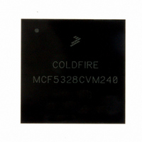
MCF5328CVM240 Freescale Semiconductor, MCF5328CVM240 Datasheet - Page 12

MCF5328CVM240
Manufacturer Part Number
MCF5328CVM240
Description
IC MCU 32BIT 240MHZ 256-MAPBGA
Manufacturer
Freescale Semiconductor
Series
MCF532xr
Datasheet
1.MCF5328CVM240J.pdf
(50 pages)
Specifications of MCF5328CVM240
Core Processor
Coldfire V3
Core Size
32-Bit
Speed
240MHz
Connectivity
EBI/EMI, Ethernet, I²C, SPI, SSI, UART/USART, USB, USB OTG
Peripherals
DMA, LCD, PWM, WDT
Number Of I /o
94
Program Memory Type
ROMless
Ram Size
32K x 8
Voltage - Supply (vcc/vdd)
1.4 V ~ 3.6 V
Oscillator Type
External
Operating Temperature
-40°C ~ 85°C
Package / Case
256-MAPBGA
Program Memory Size
16KB
Cpu Speed
240MHz
Embedded Interface Type
CAN, I2C, MAC, Ethernet, QSPI, UART
Rohs Compliant
Yes
Family Name
MPC5xxx
Device Core
ColdFire
Device Core Size
32b
Frequency (max)
240MHz
Instruction Set Architecture
RISC
Supply Voltage 1 (typ)
1.8/2.5/3.3V
Operating Supply Voltage (max)
1.6/1.95/2.75/3.6V
Operating Supply Voltage (min)
1.4/1.7/2.25/3V
Operating Temp Range
-40C to 85C
Operating Temperature Classification
Industrial
Mounting
Surface Mount
Pin Count
256
Package Type
MA-BGA
Lead Free Status / RoHS Status
Lead free / RoHS Compliant
Eeprom Size
-
Program Memory Size
-
Data Converters
-
Lead Free Status / Rohs Status
Compliant
Available stocks
Company
Part Number
Manufacturer
Quantity
Price
Company:
Part Number:
MCF5328CVM240
Manufacturer:
FREESCAL
Quantity:
717
Company:
Part Number:
MCF5328CVM240
Manufacturer:
Freescale Semiconductor
Quantity:
10 000
Part Number:
MCF5328CVM240
Manufacturer:
FREESCALE
Quantity:
20 000
Company:
Part Number:
MCF5328CVM240J
Manufacturer:
Freescale Semiconductor
Quantity:
10 000
Pin Assignments and Reset States
12
1
2
3
4
5
6
7
8
Refers to pin’s primary function.
Pull-up enabled internally on this signal for this mode.
The SDRAM functions of these signals are not programmable by the user. They are dynamically switched by the processor
when accessing SDRAM memory space and are included here for completeness.
Primary functionality selected by asserting the DRAMSEL signal (SDR mode). Alternate functionality selected by negating
the DRAMSEL signal (DDR mode). The GPIO module is not responsible for assigning these pins.
GPIO functionality is determined by the edge port module. The GPIO module is only responsible for assigning the alternate
functions.
If JTAG_EN is asserted, these pins default to Alternate 1 (JTAG) functionality. The GPIO module is not responsible for
assigning these pins.
Pull-down enabled internally on this signal for this mode.
Must be left floating for proper operation of the PLL.
Signal Name
PLL_TEST
USB_VDD
USB_VSS
PLL_VDD
PLL_VSS
SD_VDD
PST[3:0]
TEST
EVDD
IVDD
VSS
7
8
Table 3. MCF5327/8/9 Signal Information and Muxing (continued)
GPIO
—
—
—
—
—
—
—
—
—
—
—
MCF532x ColdFire
Alternate 1
—
—
—
—
—
—
—
—
—
—
—
®
Power Supplies
Alternate 2
Microprocessor Data Sheet, Rev. 5
—
—
—
—
—
—
—
—
—
—
—
Test
—
—
—
—
—
—
—
—
O
I
I
EVDD
EVDD
EVDD
—
—
—
—
—
—
—
—
E5, K5, K10,
N8, P8, L9,
F5–F7, H9,
H6–H8, P9
J8, J9, K8,
MAPBGA
J5–J7, K7
MCF5327
F8–F10,
K9, K11
G6–G9,
E6, E7,
E8, E9,
H10
G10
H11
H12
E10
196
J10
M9
—
E5, G12, M5,
L9–L11, M9,
E9, F9–F11,
G5, G6, H5,
E8, F5–F8,
J5, J6, K5,
K6, L5–L8,
MAPBGA
M11, M12
G11, H11,
MCF5328
R10, T10,
K11, K12,
R11, T11
G7–G10,
H7–H10,
L12, L13
H6, J11,
K7–K10,
M6, M7
J7–10,
Freescale Semiconductor
M10
M14
A16
N13
K13
256
J12
L14
E5, G12, M5,
L9–L11, M9,
E9, F9–F11,
G5, G6, H5,
MCF53281
E8, F5–F8,
J5, J6, K5,
K6, L5–L8,
M11, M12
G11, H11,
MCF5329
MAPBGA
R10, T10,
K11, K12,
R11, T11
G7–G10,
H7–H10,
L12, L13
H6, J11,
K7–K10,
M6, M7
J7–10,
M10
M14
A16
N13
K13
256
J12
L14


