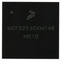
MCF5253CVM140 Freescale Semiconductor, MCF5253CVM140 Datasheet - Page 19

MCF5253CVM140
Manufacturer Part Number
MCF5253CVM140
Description
IC MPU 32BIT 140MHZ 225-MAPBGA
Manufacturer
Freescale Semiconductor
Series
MCF525xr
Datasheets
1.MCF5253VM140J.pdf
(34 pages)
2.MCF5253VM140J.pdf
(8 pages)
3.MCF5253VM140J.pdf
(648 pages)
4.MCF5253VM140J.pdf
(2 pages)
Specifications of MCF5253CVM140
Core Processor
Coldfire V2
Core Size
32-Bit
Speed
140MHz
Connectivity
CAN, EBI/EMI, I²C, QSPI, UART/USART, USB OTG
Peripherals
DMA, WDT
Program Memory Type
ROMless
Ram Size
128K x 8
Voltage - Supply (vcc/vdd)
1.08 V ~ 1.32 V
Data Converters
A/D 6x12b
Oscillator Type
External
Operating Temperature
-40°C ~ 85°C
Package / Case
225-MAPBGA
Family Name
MCF5xxx
Device Core
ColdFire V2
Device Core Size
32b
Frequency (max)
140MHz
Instruction Set Architecture
RISC
Supply Voltage 1 (typ)
1.2/3.3V
Operating Supply Voltage (max)
1.32/3.6V
Operating Supply Voltage (min)
1.08/3V
Operating Temp Range
-40C to 85C
Operating Temperature Classification
Industrial
Mounting
Surface Mount
Pin Count
225
Package Type
MA-BGA
Lead Free Status / RoHS Status
Lead free / RoHS Compliant
Number Of I /o
-
Eeprom Size
-
Program Memory Size
-
Lead Free Status / Rohs Status
Compliant
Available stocks
Company
Part Number
Manufacturer
Quantity
Price
Company:
Part Number:
MCF5253CVM140
Manufacturer:
FREESCALE
Quantity:
300
Company:
Part Number:
MCF5253CVM140
Manufacturer:
Freescale Semiconductor
Quantity:
10 000
Part Number:
MCF5253CVM140
Manufacturer:
FREESCALE
Quantity:
20 000
Company:
Part Number:
MCF5253CVM140J
Manufacturer:
Freescale Semiconductor
Quantity:
10 000
5
Table 18
later time.
6
This section includes the pin assignment information, contact connection diagram, and the mechanical
package drawing.
Freescale Semiconductor
J2A
J2B
J3A
J3B
J10
J11
J12
ID
J1
J4
J5
J6
J7
J8
J9
–
Power Consumption
Package Information and Pinout
shows maximum power consumption for the MCF5253 device. Typicals will be supplied at a
TCK Frequency of Operation
TCK Cycle Time
TCK Clock Pulse High Width
TCK Clock Pulse Low Width
TCK Fall Time (V
TCK Rise Time (V
TDI, TMS to TCK rising (Input Setup)
TCK rising to TDI, TMS Invalid (Hold)
Boundary Scan Data Valid to TCK (Setup)
TCK to Boundary Scan Data Invalid to rising edge (Hold)
TRST Pulse Width (asynchronous to clock edges)
TCK falling to TDO Valid (signal from driven or three-state)
TCK falling to TDO High Impedance
TCK falling to Boundary Scan Data Valid (signal from driven or three-state)
TCK falling to Boundary Scan. Data High Impedance
1
MCF5253 ColdFire Processor Data Sheet: Technical Data, Rev. 4
IH
(with core supplied via internal 1.2 V regulator
IL
=2.4 V to V
This does not include the current required for any externally
connected 3.3V device (e.g., flash, SDRAM, and other I/O
devices).
=0.5 v to V
which is fed from the 3.3 V supply)
(with core supplied separately)
Table 18. Maximum Power Consumption
IL
IH
Table 17. JTAG Timing Parameters
=0.5 V)
=2.4 V)
Characteristic
1.2 V Core
3.3 V I/O
3.3 V I/O
Supply
Maximum Current
150 mA
150 mA
400 mA
1
Min
100
25
25
10
10
12
—
—
—
—
0
8
1
2
1
Power Consumption
Max
10
15
15
—
—
—
—
—
—
—
—
15
15
5
5
Units
MHz
ns
ns
ns
ns
ns
ns
ns
ns
ns
ns
ns
ns
ns
ns
19


