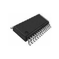
SP3243ECA-L Exar Corporation, SP3243ECA-L Datasheet - Page 10

SP3243ECA-L
Manufacturer Part Number
SP3243ECA-L
Description
IC TXRX RS232 INTELLIGENT 28SSOP
Manufacturer
Exar Corporation
Type
Transceiverr
Specifications of SP3243ECA-L
Package / Case
28-SSOP (0.200", 5.30mm Width)
Number Of Drivers/receivers
3/5
Protocol
RS232
Voltage - Supply
3 V ~ 5.5 V
Mounting Type
Surface Mount
Operating Supply Voltage
3 V to 5.5 V
Supply Current
0.3 mA
Operating Temperature Range
0 C to + 70 C
Mounting Style
SMD/SMT
Lead Free Status / RoHS Status
Lead free / RoHS Compliant
Lead Free Status / RoHS Status
Lead free / RoHS Compliant, Lead free / RoHS Compliant
Other names
1016-1120-5
Available stocks
Company
Part Number
Manufacturer
Quantity
Price
Company:
Part Number:
SP3243ECA-L
Manufacturer:
Atmel
Quantity:
27
Part Number:
SP3243ECA-L
Manufacturer:
SIPEX/EXAR
Quantity:
20 000
Charge Pump
The charge pump is a Exar–patented design
(U.S. 5,306,954) and uses a unique approach
compared to older less–efficient designs.
The charge pump still requires four external
capacitors, but uses a four–phase voltage
shifting technique to attain symmetrical 5.5V
power supplies. The internal power supply
consists of a regulated dual charge pump that
provides output voltages 5.5V regardless of
the input voltage (V
range. This is important to maintain compli-
ant RS-232 levels regardless of power supply
fluctuations.
The charge pump operates in a discontinuous
mode using an internal oscillator. If the output
voltages are less than a magnitude of 5.5V, the
charge pump is enabled. If the output voltages
exceed a magnitude of 5.5V, the charge pump
is disabled.
phases of the voltage shifting. A description of
each phase follows.
Phase 1
— V
clock cycle, the positive side of capacitors C
C
to GND and the charge in C
Since C
across capacitor C
Phase 2
— V
connects the negative terminal of C
storage capacitor and the positive terminal of
C
ated voltage to C
regulated to a minimum voltage of -5.5V.
Simultaneous with the transfer of the voltage to C
the positive side of capacitor C
and the negative side is connected to GND.
Phase 3
— V
clock is identical to the first phase — the charge
transferred in C
terminal of C
side of capacitor C
age potential across C
2
2
are initially charged to V
to GND. This transfers a negative gener-
SS
DD
SS
charge storage — During this phase of the
charge storage — The third phase of the
2
+
transfer — Phase two of the clock
is connected to V
1
, which is applied to the negative
This oscillator controls the four
Exar Corporation 48720 Kato Road, Fremont CA, 94538 • 510-668-7017 • www.exar.com
1
produces –V
3
2
2
. This generated voltage is
. Since C
CC
is now 2 times V
) over the +3.0V to +5.5V
2
is 2 times V
CC
CC
1
–
, the voltage potential
. C
is transferred to C
2
+
1
CC
is at V
l
is switched to V
+
is then switched
in the negative
CC
2
CC
CC
.
to the V
.
, the volt-
1
and
2
CC
SS
–
3
.
,
10
Phase 4
— V
connects the negative terminal of C
and transfers this positive generated voltage
across C
voltage is regulated to +5.5V. At this voltage,
the internal oscillator is disabled. Simultane-
ous with the transfer of the voltage to C
positive side of capacitor C
and the negative side is connected to GND, al-
lowing the charge pump cycle to begin again.
The charge pump cycle will continue as long
as the operational conditions for the internal
oscillator are present.
Since both V
from V
be symmetrical. Older charge pump approaches
that generate V
the magnitude of V
inherent inefficiencies in the design. The clock
rate for the charge pump typically operates at
greater than 250kHz. The external capacitors
can be as low as 0.1µF with a 16V breakdown
voltage rating.
DD
CC
transfer — The fourth phase of the clock
, in a no–load condition V
2
to C
+
4
and V
, the V
–
from V
–
–
compared to V
DD
are separately generated
+
storage capacitor. This
will show a decrease in
1
is switched to V
SP3243E_101_111009
+
+
and V
2
due to the
to GND,
4
, the
–
will
CC


