TWR-K60N512-KIT Freescale Semiconductor, TWR-K60N512-KIT Datasheet - Page 8
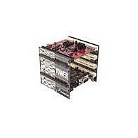
TWR-K60N512-KIT
Manufacturer Part Number
TWR-K60N512-KIT
Description
TOWER SYSTEM KIT K60N512
Manufacturer
Freescale Semiconductor
Series
Kinetisr
Type
MCUr
Specifications of TWR-K60N512-KIT
Contents
4 Boards, Documentation, DVD
Processor To Be Evaluated
K60
Data Bus Width
32 bit
Interface Type
RS-232, USB, CAN, I2C, SPI, UART
Dimensions
3.5 in x 3.5 in x 3.5 in
Operating Supply Voltage
1.71 V to 3.6 V
Silicon Manufacturer
Freescale
Core Architecture
ARM
Core Sub-architecture
Cortex - M4
Silicon Core Number
MK
Silicon Family Name
Kinetis - K60
Kit Contents
4x Brds, Cable, Docs
Rohs Compliant
Yes
For Use With/related Products
Freescale Tower System, K60N512
Lead Free Status / RoHS Status
Lead free / RoHS Compliant


2.2 Clocking
The Kinetis MCUs start up from an internal digitally controlled oscillator (DCO). Software can enable
one or two external oscillators if desired. The external oscillator for the Multipurpose Clock Generator
(MCG) module can range from 32.768 KHz up to a 32 MHz crystal or ceramic resonator. The external
oscillator for the Real Time Clock (RTC) module accepts a 32.768 kHz crystal.
The EXTAL pin of the main external oscillator can also be driven directly from an external clock source.
The TWR-K60N512 features a 50 MHz on-board clock oscillator as seen in sheet 4 of the schematics.
However, when the K60 Ethernet MAC is operating in RMII mode, synchronization of the MCU input
clock and the 50 MHz RMII transfer clock is important. In this mode, the MCU input clock must be kept
in phase with the 50 MHz clock supplied to the external PHY. Therefore, the TWR-K60N512 provides
the option (see description for J6 in Table 5) to select the clock input to the MCU from 1) the on-board
50MHz source or 2) an external clock from the CLKIN0 pin on the Primary Connector. When the K60 is
operating in Ethernet RMII mode, the Tower peripheral module implementing the RMII PHY device
should drive a 50 MHz clock on the CLKIN0 signal that is kept in phase with the clock supplied to the
RMII PHY. Refer to section 2.10 “Ethernet” for more information.
2.3 System Power
In stand-alone operation, the main power source for the TWR-K60N512 module is derived from the
5.0V input from either the USB mini-B connector, J13, or the debug header, J11, when a shunt is placed
on jumper J12. A low-dropout regulator provides a 3.3V supply from the 5.0V input voltage. Refer to
sheet 5 of the TWR-K60N512 schematics for more details.
When installed into a Tower System, the TWR-K60N512 can be powered from either an on-board
source or from another source in the assembled Tower System. If both the on-board and off-board
sources are available, the TWR-K60N512 will default to the off-board source.
The 3.3V power supplied to the MCU is routed through a jumper, J8. The jumper shunt can be removed
to allow for either 1) alternate MCU supply voltages to be injected or 2) the measurement of power
consumed by the MCU.
2.3.1 RTC VBAT
The Real Time Clock (RTC) module on the K60 has two modes of operation, system power-up and
system power-down. During system power-down, the RTC is powered from the backup power supply,
High-speed analog comparator with 6-bit DAC
Programmable voltage reference
USB full-speed/low-speed OTG/Host/Device controller with device charge detect
10/100 Mbps Ethernet MAC
SPI, I
SD Host Controller (SDHC)
GPIO with pin interrupt support, DMA request capability, digital glitch filtering
Capacitive touch sensing inputs (TSI)
Debug interfaces: JTAG, cJTAG, SWD
Trace: TPIO, FPB, DWT, ITM, ETM, ETB
2
C (w/ SMBUS support), UART (w/ ISO7816 and IrDA), CAN, I
TWR-K60N512 Tower Module User's Manual
2
S
Page 8 of 17
Related parts for TWR-K60N512-KIT
Image
Part Number
Description
Manufacturer
Datasheet
Request
R

Part Number:
Description:
Manufacturer:
Freescale Semiconductor, Inc
Datasheet:
Part Number:
Description:
Manufacturer:
Freescale Semiconductor, Inc
Datasheet:
Part Number:
Description:
Manufacturer:
Freescale Semiconductor, Inc
Datasheet:
Part Number:
Description:
Manufacturer:
Freescale Semiconductor, Inc
Datasheet:
Part Number:
Description:
Manufacturer:
Freescale Semiconductor, Inc
Datasheet:
Part Number:
Description:
Manufacturer:
Freescale Semiconductor, Inc
Datasheet:
Part Number:
Description:
Manufacturer:
Freescale Semiconductor, Inc
Datasheet:
Part Number:
Description:
Manufacturer:
Freescale Semiconductor, Inc
Datasheet:
Part Number:
Description:
Manufacturer:
Freescale Semiconductor, Inc
Datasheet:
Part Number:
Description:
Manufacturer:
Freescale Semiconductor, Inc
Datasheet:
Part Number:
Description:
Manufacturer:
Freescale Semiconductor, Inc
Datasheet:
Part Number:
Description:
Manufacturer:
Freescale Semiconductor, Inc
Datasheet:
Part Number:
Description:
Manufacturer:
Freescale Semiconductor, Inc
Datasheet:
Part Number:
Description:
Manufacturer:
Freescale Semiconductor, Inc
Datasheet:
Part Number:
Description:
Manufacturer:
Freescale Semiconductor, Inc
Datasheet: